Memory banks
Memory banks are freely accessible memory areas in which device-specific information and properties can be stored. The contents of the memory banks can be read with FB_DALI10xReadMemoryLocation (see FB_DALI102ReadMemoryLocation and FB_DALI103ReadMemoryLocation) and, if enabled, written with FB_DALI10xWriteMemoryLocationNoReply (see FB_DALI102WriteMemoryLocationNoReply and FB_DALI103WriteMemoryLocationNoReply).
Part of the memory banks can be provided with write protection.
A DALI device can support a maximum of 256 memory banks, each with up to 255 bytes, with memory banks 200 to 255 being reserved. Memory bank 0 and memory bank 1 are predefined by IEC 62386.
Structure of memory bank 0:
Memory bank 0 is read only and contains general, vendor-specific information about the DALI control gear or DALI control device. Every certified DALI device must implement memory bank 0. Up to offset 16#1A the fields are defined by IEC 62386 as follows.
Offset | Description | Default values |
|---|---|---|
16#00 | Offset of the last memory area inside the memory bank that can be accessed. | Vendor-specific |
16#01 | Reserved, not implemented |
|
16#02 | Number of the last memory bank that can be accessed. | Vendor-specific |
16#03 | GTIN byte 0 (MSB) | Vendor-specific |
16#04 | GTIN byte 1 | Vendor-specific |
16#05 | GTIN byte 2 | Vendor-specific |
16#06 | GTIN byte 3 | Vendor-specific |
16#07 | GTIN byte 4 | Vendor-specific |
16#08 | GTIN byte 5 (LSB) | Vendor-specific |
16#09 | Firmware Version (major) | Vendor-specific |
16#0A | Firmware Version (minor) | Vendor-specific |
16#0B | Identification number byte 0 (MSB) | Vendor-specific |
16#0C | Identification number byte 1 | Vendor-specific |
16#0D | Identification number byte 2 | Vendor-specific |
16#0E | Identification number byte 3 | Vendor-specific |
16#0F | Identification number byte 4 | Vendor-specific |
16#10 | Identification number byte 5 | Vendor-specific |
16#11 | Identification number byte 6 | Vendor-specific |
16#12 | Identification number byte 7 (LSB) | Vendor-specific |
16#13 | Hardware version (major) | Vendor-specific |
16#14 | Hardware version (minor) | Vendor-specific |
16#15 | 101 Version number of the current DALI standard | Vendor-specific |
16#16 | 102 Version numbers of all integrated DALI control gears | Vendor-specific |
16#17 | 103 Version numbers of all integrated DALI control devices | Vendor-specific |
16#18 | Number of logical control units in the device | Vendor-specific |
16#19 | Number of logical control gears in the device | Vendor-specific |
16#1A | Index number of this logical DALI control gear or DALI control device | Vendor-specific |
16#1B…16#7F | Reserved, not implemented |
|
16#80…16#FE | Additional device information | Vendor-specific |
16#FF | Reserved, not implemented |
|
Structure of memory bank 1:
Memory bank 1 can be used by the device vendor to store further information in the DALI device. Up to offset 16#10 the fields are defined by IEC 62386 as follows.
Offset | Description | Default values | Memory |
|---|---|---|---|
16#00 | Offset of the last memory area inside the memory bank that can be accessed. | Vendor-specific (16#10…16#FE) |
|
16#01 | Indicator byte | Vendor-specific |
|
16#02 | Lock byte for memory bank 1. Writeable bytes become changeable through the value 16#55. No other values make writing possible. | 16#FF |
|
16#03 | OEM GTIN byte 0 (MSB) | 16#FF | Lockable by byte 16#02 |
16#04 | OEM GTIN byte 1 | 16#FF | Lockable by byte 16#02 |
16#05 | OEM GTIN byte 2 | 16#FF | Lockable by byte 16#02 |
16#06 | OEM GTIN byte 3 | 16#FF | Lockable by byte 16#02 |
16#07 | OEM GTIN byte 4 | 16#FF | Lockable by byte 16#02 |
16#08 | OEM GTIN byte 5 (LSB) | 16#FF | Lockable by byte 16#02 |
16#09 | OEM Identification number byte 0 (MSB) | 16#FF | Lockable by byte 16#02 |
16#0A | OEM Identification number byte 1 | 16#FF | Lockable by byte 16#02 |
16#0B | OEM Identification number byte 2 | 16#FF | Lockable by byte 16#02 |
16#0C | OEM Identification number byte 3 | 16#FF | Lockable by byte 16#02 |
16#0D | OEM Identification number byte 4 | 16#FF | Lockable by byte 16#02 |
16#0E | OEM Identification number byte 5 | 16#FF | Lockable by byte 16#02 |
16#0F | OEM Identification number byte 6 | 16#FF | Lockable by byte 16#02 |
16#10 | OEM Identification number byte 7 (LSB) | 16#FF | Lockable by byte 16#02 |
16#11…16#FE | Additional device information | Vendor-specific |
|
16#FF | Reserved, not implemented |
|
|
Structure of memory banks 2 to 199:
The device vendor can use memory banks 2 to 199 to supply further parameters. The structure of the memory banks is always as shown below. The vendor of the DALI device must be consulted regarding the contents and the possibility to write individual bytes.
Offset | Description | Default values | Memory |
|---|---|---|---|
16#00 | Offset of the last memory area inside the memory bank that can be accessed. | Vendor-specific (16#03…16#FE) |
|
16#01 | Indicator byte | Vendor-specific |
|
16#02 | Lock byte for the memory bank. Writeable bytes become changeable through the value 16#55. No other values make writing possible. | 16#FF |
|
16#03…16#FE | Additional device information | Vendor-specific | Vendor-specific; lockable by byte 16#02 if enabled by the vendor |
16#FF | Reserved, not implemented |
|
|
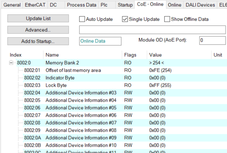
Access to memory bank 2 on the EL6821
Since the KL6821/EL6821 represents a DALI control device according to IEC 62386, the Bus Terminal must offer memory bank 0 and memory bank 1. Other DALI control devices can access these memory banks via the corresponding DALI commands.
In addition, the EL6821 offers memory bank 2. In the EL6821 memory bank 2 is mapped by CoE object 16#8002. The first three fields (16#8002:01 ... 16#8002:03) are defined by IEC 62386 (see above). The fields 16#8002:04 to 16#8002:FF can be written and/or read individually.
Note that the offset in memory bank 2 and the subindex are shifted from the CoE. Thus, offset 10 in memory bank 2 corresponds to field 16#8002:0B.
The function blocks FB_DALI102ReadMemoryLocation/FB_DALI103ReadMemoryLocation or FB_DALI102WriteMemoryLocationNoReply/FB_DALI103WriteMemoryLocationNoReply are available for accessing the memory banks of a DALI device via the DALI bus.
If memory bank 2 of the own EL6821 is to be accessed from a PLC program, access is via the EtherCAT CoE interface. The TwinCAT library Tc2_EtherCAT offers the necessary function blocks for this (see FB_EcCoeSdoRead and FB_EcCoeSdoWrite).
The following example reads offset 3 (subindex 4) and writes offset 4 (subindex 5) of memory bank 2. The EL6821 must be located at the same controller where the PLC program is executed.
VAR
  fbCoERead      : FB_EcCoESdoRead;
  fbCoEWrite     : FB_EcCoESdoWrite;
  nValue         : USINT;
  bExecuteRead   : BOOL;
  bExecuteWrite  : BOOL;
END_VAR
fbCoERead(sNetId := F_CreateAmsNetId(GVL.stEL6821InData01.stAdsAddr.netId),
nSlaveAddr := GVL.stEL6821InData01.stAdsAddr.port,
nIndex := 16#8002,
nSubIndex := 16#04,
pDstBuf := ADR(nValue),
cbBufLen := SIZEOF(nValue),
bExecute := bExecuteRead);
IF (NOT fbCoERead.bBusy) THEN
bExecuteRead := FALSE;
END_IF
fbCoEWrite(sNetId := F_CreateAmsNetId(GVL.stEL6821InData01.stAdsAddr.netId),
nSlaveAddr := GVL.stEL6821InData01.stAdsAddr.port,
nIndex := 16#8002,
nSubIndex := 16#05,
pSrcBuf := ADR(nValue),
cbBufLen := SIZEOF(nValue),
bExecute := bExecuteWrite);
IF (NOT fbCoEWrite.bBusy) THEN
bExecuteWrite := FALSE;
END_IF