Current control trigger pulse
In pulse mode, the maximum current amplitude is 3 A with 12 V LEDs.
The specific parameters for setting the LED output as a trigger-controlled pulse output are described below. In order to generate a reproducible behavior at the LED output via a signal at the trigger input, the signal at the trigger input should have a steep edge.
For all pulsed operating modes (current control timestamp pulse, current control trigger pulse, current control PLC pulse) the maximum constant duty cycle as a function of the output current must be considered.
- Iout = 1 A: 20% duty cycle
- Iout = 2 A: 10% Duty Cycle
- Iout = 3 A: 8% Duty Cycle
In this operation mode, it is possible to configure the trigger input as an enable input so that it can be used as an external switch. An output can then only be actuated with a specified signal at the trigger input. The LED output then switches synchronously with the signal at the trigger input. More detailed information and commissioning can be found in the chapter Hardware enable. Alternatively, the trigger input is used as a trigger input, so that a pulse with a specified delay, duration and current is output at the LED output after a signal at the trigger input.
Especially in the current controlled pulse operation modes the use of the automatic determination of the output voltage is recommended, because possibly for the generation of high current pulses at the output a high pre-voltage is needed to generate steep edges. These may be higher than voltages specified in the LED data sheet.
If the supply voltage is removed during operation in the pulsing modes, there will be a malfunction at the output. In addition, an overcurrent may occur at the LED output. Therefore, a stable voltage supply must be ensured. To minimize the risk of malfunction and overcurrent, the enable bit can be set together with the output bit so that the enable is not permanently set.
For delay-free triggering, it is recommended to trigger by PLC or internally via distributed clocks.
When using an external trigger, it should be noted that, based on internal terminal delays, the minimum delay between the trigger input and the signal output is approximately 2 µs. The offset of 2 µs must also be observed for all set delay values (regardless of whether they are set via PDO or CoE). The resulting delay is always

In the hardware versions 01 and 02 and firmware versions <FW04, oscillations of the voltage can occur at the trigger input due to the line inductance of the connected line. This can lead to incorrect detection of pulses, which causes pulses to be output at the LED output. This problem can be minimized by a resistance of approx. 1 kΩ between the trigger signal and pin 5 (TrigIn+).
From FW04, the CoE parameter 0x8004:09 “Trigger input blind time” has an adjustable waiting time for signal detection at the trigger input. The inactive time of the trigger input from the trigger start time to the end of the pulse output plus "Trigger input blind time" is adjustable in the range of 20..65535 µs. This allows interference to be intercepted.
From HW03, asynchronous interference is also filtered by the hardware.
The function "trigger input blind time" can not only be used to eliminate disturbances, but also as a kind of "dead time" to preset a fixed duty cycle, so that there is no reaction at the output even if events occur at the trigger input to protect the terminal and the LED from overheating.
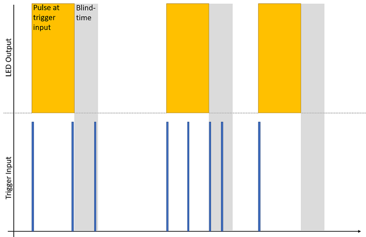 Fig.158: Behavior with "trigger input blind time"
Example: The configuration specifies a pulse length of 500 µs, a pulse delay in relation to the trigger input of 0 µs and a blind time of 150 µs. The first pulse at the trigger input is detected, as shown in the figure, and a pulse with the specified values is triggered at the LED output. During this time possible further edges at the trigger input are "ignored". After the 500 µs pulse at the LED output, the blind time begins, which is specified with 150 µs as an example. During these 150 µs, edges at the trigger input continue to be ignored. This means that no new pulses can be generated for a total of 650 µs. Only 650 µs after the first edge that triggered the pulse at the output, the trigger input reacts again to new edges (in the example the 4th edge at the trigger input). Then the same starts from the beginning. During the entire blind time, the edges are not stored.
Make the following settings:
- Nominal/limit current of the LED in the unit mA in the CoE parameter 0x8000:02 “Target current”
- Input voltage in the unit 0.01 V in the parameter 0x8000:03 “Supply voltage”
- Desired output voltage in the unit 0.01 V (max. UIN - 2 V) in the parameter 0x8000:04 “Output voltage”.
- If currents are to be output above the nominal current of the LED, a higher specification is necessary for the output voltage in the CoE parameter 0x8000:04 due to the non-linear behavior of LEDs and the current control capability of the circuit.
- In this operation mode, the value set here corresponds to the output on the controller. If the forward voltage of the connected LED is lower than the value set here, the remaining voltage drops internally in the EL2596. In many cases, this leads to overtemperature in the terminal and thus to the switching off of the LED output. As the desired output voltage, therefore, the forward voltage at the desired output current should be set here. The TeachIn function can also be used to determine the output voltage.
- Set the operation mode in the CoE directory in the parameter 0x8004:01 to “Current Control trigger pulse”
- Set “Predefined PDO Assignments” to “External trigger input (with info data)”.
- Specify the set current in the unit mA via “DOX Current” → “Output Current”.
- Specify the pulse length in the unit µs via “DOX Impulse length” → “Impulse length”. The resolution of the time can be reduced from 1 µs to 100 ns using the CoE parameter 0x8002:31 “Pulse resolution 100 ns”.
- Specify the trigger signal delay in the unit µs via “DOX Trigger delay” → “Trigger delay”. The resolution of the time can be reduced from 1 µs to 100 ns using the CoE parameter 0x8002:31 “Pulse resolution 100 ns”. Alternatively, the delay can be firmly specified in the unit 0.1 µs in the CoE parameter 0x8000:0B. If the delay is specified both in the PDOs and in the CoE parameters, these values are added together and the delay is the sum of the two.
- In the CoE parameter 0x8002:30, choose whether the LED pulse should be generated by a rising or falling edge on the trigger input.
- In the CoE parameter 0x8004:03, specify the level at the trigger input at which the LED output should be switched (high = 24 V, low = 5 V).
- Connect the trigger signal to the “TrigIn+” (5) and “TrigIn-“ (13) connections.
- Activate the trigger input under “DOX Control” → “Control” → “Input Trigger Enable”
- Check under “DOX Status” → “Status” whether the “Ready to activate” bit is 1.
- Activate the control under “DOX Control” → “Control” via the “Enable” bit.
- Switch on the LED output under “DOX Control” → “Control” by activating the “Output” bit.
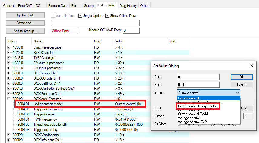 Fig.159: Operation mode setting “Current control trigger pulse”
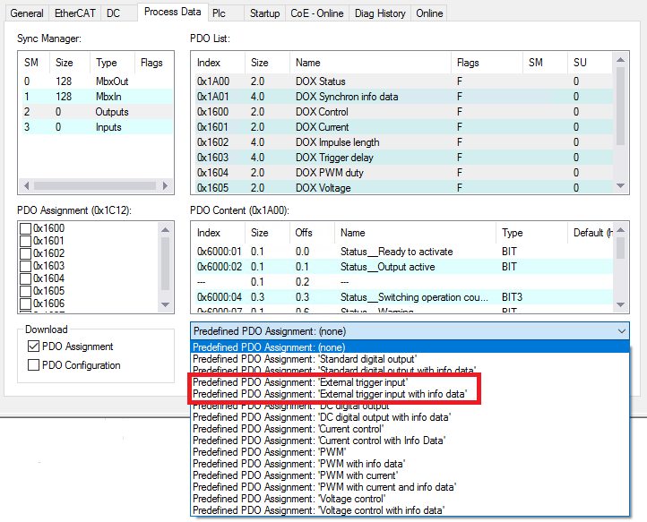 Fig.160: PDO setting “External trigger pulse (with info data)”
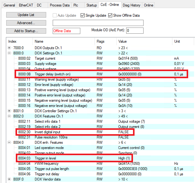 Fig.161: Settings in the CoE objects for the operation mode “Current control trigger pulse”
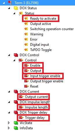 Fig.162: Activating the output in the operation mode “Current control trigger pulse”