On the mutual influence of non-isolated differential channels
This section assumes the following chapters as prior knowledge
- "Explanation of electrically (un)isolated channels"
- "Ground reference: single-ended/differential typification"
- "Explanation of the term GND/Ground"
In the following, we will further deal with the channels that are not isolated in the device and that are fed with signals with a common ground (PGND). The common ground of the connected channels (accessible from the outside, if necessary) and the differential measurement namely generate an electrical phenomenon that must be controlled on the application side by a short calculation to ensure that the device can do what it is expected to do - especially if high-precision measurement technology of the ELM3xxx series (or equivalent Beckhoff measuring devices as EPP35xx) is involved, i.e. with the claim of lowest measurement uncertainty.
Note: (High impedance) voltage measurement specifically is focused on here, for explanations on current measurement refer to the chapter Ground reference: single-ended/differential typification.
In addition, a detailed insight into the differential inner workings, taking the example of a circuit with two unisolated channels:
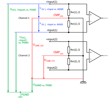
Let Rin be the input resistance of the channel (see device documentation, input impedance/internal resistance specification). In real terms, it consists of two resistances with Rin/2 each. The two resistances form a voltage divider for the respective channel and actually define the respective CMP (CommonMode-Point) with its voltage UCMP, ch vs. AGND, depending on which voltage
is applied externally via +Input/ -Input. The CMP is the channel local AGND. However, since all AGND are related, all voltages and therefore all voltages applied to +input/-input are involved in the AGND definition!
Because it must become: UCMP, ch1 = UCMP, ch2 = ... = AGND.
Knowledge of the final potential level of AGND is important for assessing whether specified application limits are exceeded, because each channel will have its own, possibly unbalanced voltage differences Uch(n), +/-input vs. Set AGND! Due to the AGND shift, even an outgoing voltage on an unconnected channel can be measurable, which is also loadable to a limited extent (source resistance is then half the input resistance).
However, this topic, which seems complex at first glance, can be approached quite easily and thus a high degree of operational reliability can be achieved with the low-cost, unisolated differential channels. The following procedure is recommended:
- Calculate UAGND referred to UPGND
PGND (system ground, supply) is selected as reference level for the above reasons, - Calculate all inputs on potential difference to AGND in use
(for steps two and three see calculation table below),
→ download - Check for exceeding the specification.
Regarding 1: calculation of AGND
UAGND can be calculated as a weighted average of the external voltages, where the weighting factors are the electrical conductances (reciprocals of the input resistances) of the individual inputs to AGND. For DC voltages:
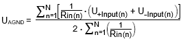 .
.
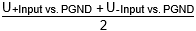
Note: n is the channel index and goes from 1 to the last connected channel N. All voltages U are referenced to PGND. If the internal resistances of all inputs are (theoretically) equal, the simplified result for UAGND is the average value of all input voltage differences:
 .
.
With some measurement modules the internal analog ground AGND is externally accessible. The voltage can be measured easily there. Care must be taken that the measuring device used (in the typical case a multimeter) does not distort the voltage UAGND by its own internal resistance!
A selection:
ELM3502‑00x0, ELM3504‑00x0, EPP3504‑0023 | Via the –Uv connection on the push-in socket |
ELM314x‑00x0 | Via Up-. For this, the setting "Connect Up- to GNDA" in the CoE (F800:01) must be set to TRUE. |
ELM334x‑00x0 | Via the AGND connection (5 and 6) to the push-in sockets |
Regarding 2: calculation inputs
After we have learned about UAGND, the max. permissible voltages or the voltages at the connection contacts are to be calculated.
Steps two and three can easily be performed using this sample table
→ download:
Regarding 3: testing
The results are to be compared with the specification limits according to the documentation with respect to
- usage limit: "max. permitted voltage during specified normal operation",
- destruction limit: "dielectric strength – destruction limit"
Notes:
- As can be seen from the steps above, changes at the inputs usually result in a change to AGND, regardless of whether the signal +input and -input change uniformly (same magnitude, same sign) (common mode influence, CommonMode) or separately. An influence of the other channels will always be visible in the measured values at high magnification.
Exception: if +input changes by the opposite amount to -input, then the CMP of the channel and its influence on the other channels remains unchanged - these explanations concern differential channels. Single-ended channels, on the other hand, are connected at one end to a signal ground (which need not necessarily be PGND) and are thus inevitably coupled to one another; depending on the wiring, AC crosstalk can be observed. An AGND shift in the device also occurs here, but since AGND is usually not accessible in these devices, this represents the normal operation of the device and is covered by the specification.
Cf. the Beckhoff definition of "SingleEnded" in chapter "Ground reference: single-ended/differential typification"
Here are a few examples 1):
- Example 1:
ELM3004-0000, all channels in U ±10 V mode, all negative inputs (–Input) connected to PGND (external reference potential) (single-ended operation), channel 1 measures +10 V, all other channels –10 V, Rin = 4.1 MΩ - Usage limit: typ. ±12.5 V against –Uv (AGND)
- According to equation: VAGND = –2.5 V
- V+Input(1), AGND = +10 V−(−2.5 V) = +12.5 V OK
V-Input(1), AGND = 0 V−(−2.5 V) = +2.5 V OK
V+Input(2), AGND = −10 V−(−2.5 V) = −7.5 V OK
V-Input(2), AGND = 0 V−(−2.5 V) = +2.5 V OK
V+Input(3), AGND = −10 V−(−2.5 V) = −7.5 V OK
V-Input(3), AGND = 0 V−(−2.5 V) = +2.5 V OK
V+Input(4), AGND = −10 V−(−2.5 V) = −7.5 V OK
V-Input(4), AGND = 0 V−(−2.5 V) = +2.5 V OK - Example 2:
ELM3002-0000, both channels in U ±2.5 V mode. Channel 1 measures a high-side shunt (i.e. +Input(1) to +24 V) with −300 mV, channel 2 measures a low-side shunt (i.e. -Input(2) to PGND) with +800 mV. - Usage limit: typ. ±12.5 V against –Uv (AGND)
- According to equation: VAGND = +12.125 V
- V+Input(1), AGND = +24 V−12.125 V = +11.875 V OK
V-Input(1), AGND = +23.7 V−12.125 V = +11.575 V OK
V+Input(2), AGND = 0.8 V−12.125 = −11.325 V OK
V-Input(2), AGND = 0 V−12.125 V = −12.125 V OK - Example 3:
As above, but the high-side shunt is connected to +30 V: - According to equation: VAGND = +15.125 V
- V+Input(1),AGND = +30 V − 15.125 V = +14.875 V NOK
V-Input(1),AGND = +29.7 V − 15.125 V = +14.575 V NOK
V+Input(2),AGND = 0.8 V − 15.125 = −14.325 V NOK
V-Input(2),AGND = 0 V − 15.125 V = −15.125 V NOK - Example 4:
ELM3002-0000, channel 1 in U ±30 V mode (other Rin!), channel 2 in U ±10 V mode. Both negative inputs (-Input) connected to PGND (external reference potential). Channel 1 measures +20 V, channel 2 measures +2 V:
Usage limits:
Channel 1: typ. ±35 V against -Uv (AGND), channel 2: typ. ±12.5 V against -Uv (AGND) - According to equation: VAGND = +7.816 V
- V+Input(1), AGND = +20 V – 7.816 V = +12.2 V OK
V-Input(1), AGND = 0 V − 7.816V = -7.8 V OK
V+Input(2), AGND = 2 V − 7.816V = -5.8 V OK
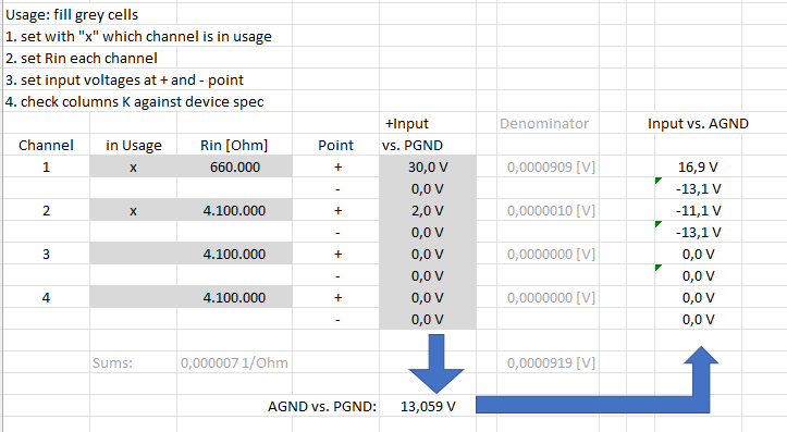
V-Input(2), AGND = 0 V − 7.816V = -7.8 V OK - Example 5:
as above, but channel 1 measures +30 V: - VAGND = +13.059 V
- V+Input(1), AGND = +30 V − 13.059 V = +16.9 V OK
V-Input(1), AGND = 0 V − 13.059 V = −13.1 V OK
V+Input(2), AGND = 2 V − 13.059 V = −11.1 V OK
V-Input(2), AGND = 0 V − 13.059 V = −13.1 V NOK
1) The values given for usage limit and Rin are to be regarded as examples; valid specification values can be found in the respective device documentation.