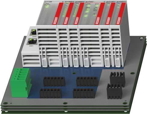
Structure of the PCB layers
Requirements of the PCB
A multilayer PCB with at least four Layers is recommended for EJ-Backplane, in order to allow complete covering of the differential pairs with copper (GND net) from both sides of the PCB.
Notice | |
Avoid damage of backplane and components! Short circuit condition has to be taken into account for cross section configuration. |
The snap in mechanism of the EJ-Modules is designed for a PCB thickness of 1.6 mm ±10%.

The following chapters show an example for a PCB with four layers with the routing in the individual layers.
Notice | |
Note on routing
|
Further Information