Function principles and notes
The EL5001/EL5002 is an SSI master terminal for cyclic polling of SSI devices. The EL5002 can operate two slaves.
The EL500x is generally operated such that each I/O cycle triggers an SSI communication and thus supplies a new encoder position to the application. If the time falls below a minimum EtherCAT cycle time that depends on the settings and the hardware, this interrelationship can no longer be guaranteed and the SSI transfers are no longer synchronous to the EtherCAT cycle and the DC cycle (see below: EtherCAT cycle time).
SSI principles
SSI communication sequence
- The SSI master starts pulsing on the clock line with a fixed cycle into the shift register of the SSI slave.
- The slave generally "pushes back" data with a width of 25 bits on the data line. An SSI encoder should determine its position with the first falling edge of the signal at the Clock input ("latching"), which is then transferred.
- Once the specified number of bits was pushed, the clock signal is terminated.
- After a pause, polling by the SSI master recommences.
The last data bit can be a PowerFail bit, i.e. the slave signals a power failure. This output depends on the slave.
The number of bit changes equals the clock frequency, i.e. the maximum data transfer rate for a 1 MHz cycle is 1 Mbit/s.
The EL500x devices have a 120 Ω termination resistor in the incoming data line.
Various parameters have to be set in the EL500x SSI master in order to ensure that the data of the SSI slave are transferred correctly:
- Baud rate (e.g. 500 kBaud)
- Coding (e.g. Gray code)
- Data frame type, e.g. multi-turn 25 bits
- Data frame size, e.g. 25 bits
- Data length, i.e. how many bits in the data frame represent the actual position data, e.g. 24 bits.
This information can be found in the data sheet for the SSI slave and must be set in the CoE directory of the EL500x.
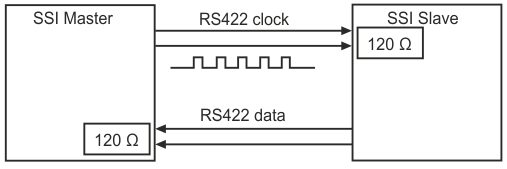 Fig.139: Schematic diagram
Referencing an SSI signal
An SSI encoder is an absolute encoder, which means, that the position value is available without referencing immediately after switching on.
Many SSI encoders offer the option of referencing or zeroing the position value via an additional digital input. Depending on the signal voltage of the digital input on the encoder, this can be set, for example via a digital output terminal EL2xxx.
EL500x functionality
Technical development enables expansion of the EL5001 functionality. The following extensions are available, depending on the hardware/firmware version:
EL5001 up to firmware (FW) 10 (up to EL5001-0000-0001)
- The master terminal starts the SSI communication only with the EtherCAT cycle, in so-called synchronous mode.
- The CoE settings (baud rate, frame length, ..) are implemented in the object directory in objects 0x4060ff.
- The process data interface consists of status (1 byte) and value (4 byte).
EL5001 from firmware (FW) 11 (from EL5001-0000-1017) and EL5002 (from EL5002-0000-0016)
- These versions feature additional distributed clock functionality and are able to poll the SSI slave precisely synchronized with other distributed clock devices. This eliminates communication-related jitter, resulting in a significant reduction of the time uncertainty.
- The CoE settings (baud rate, frame length, ..) are predominately implemented in the object library in object 0x8010 (EL5001) or 0x8000 / 0x8010 (EL5002) with its subindices.
The settings will also continue to be managed in indices 0x4060ff. Any modified settings are copied into the corresponding other section. - By default the EL500x is recognized in the known process image (status [1 byte] and value [4 byte]).
In addition an extended process image featuring 2 status bytes and 4 value bytes can be selected. From TwinCAT 2.11 the bits from the status variable can also be linked individually.
 | Firmware update Older EL5001 devices with firmware version 10 cannot be updated with later firmware! |
EL5002 from firmware (FW) 03 (from EL5002-0000-0020)
The firmware of EL5002 has been extended by the following functions:
- Improved jitter, max. ±100 ns
- Implementation of multiple transmission mode
Improved Jitter
In the DC Synchronous mode the process data handling in the slave is triggered by the hardware SYNC events, generated in the slave, based on the DC system time. The local clock in each slave is synchronized by the master to the DC system time during initialization phase. Based on DC system time, hardware SYNC events are generated within each slave.
The EL5002 trigger with the SYNC0 / SYNC1 event the SSI Clock output to the SSI slave. The triggered event has a device specific time jitter. This time jitter is optimized in the EL5002 to the value: max. ±100 ns.
The jitter compensation can be enabled for each channel individually with via object 0x80n0:0C.
Index (hex) | Name | Meaning |
|---|---|---|
Enable SSI clock jitter compensation | 0: SSI clock jitter compensation is disabled (default) | |
1: SSI clock jitter compensation is enabled |
Multiple transmission mode
The following modes can be used with the SSI protocol:
- Single transmission (already part of EL5002)
- Multiple transmission (new feature, available from FW03 and XML Rev. 0020)
The single transmission is implemented according to the SSI protocol standard. The multiple transmission is an extension of the single transmission and can be activated by the user for each channel independently.
For the multiple transmission the SSI master sends additional clock pulses / clock bursts (at least additional one) within the monoflop time. As response the complete data word, that was already transmit after the first rising clock edge, is expected. The received data values are compared. If there is a difference between the received data value, an error state indicated by an error bit is set. Therefore the multiple transmission is ideally suited to check the data integrity.
The multiple transmission can be activated by a CoE object, for each channel independently. The number of additional send clock bursts can be set by the user.
Index 0x80n0 SSI settings
Index (hex) | Name | Meaning |
|---|---|---|
Number of clock bursts | 1: single transmission is active (Default) | |
2: multiple transmission with 2 clock bursts | ||
3: multiple transmission with 3 clock bursts |
The additional clock bursts are send within the monoflop time tm, these time is specified:
- Monoflop time of encoder: 15 µs < tm < 25 µs
The multiple transmission functionality cannot be guaranteed for monoflop time tm < 15 µs.
The number of the additionally send clock bursts is restricted by the baudrate. The higher the baudrate, more clock bursts can be sent.
While during single transmission received value is directly written to the counter value, for multiple transmission the first valid value is written to the counter value. This means:
multiple transmission with 2 clock bursts (0x80n0:14):
- Both values are compared. If the values are similar, the first received value is written to the counter value. If the consecutive received values are different, the transmission failure is indicated by an error bit in the status byte (SB). The first received value, also if it is not valid, is set as counter value.
multiple transmission with 3 clock bursts (0x80n0:14):
- Three values are compared. At least two out of three values need to be similar. The first valid value is written to the counter value. If all three received values are different, the transmission failure is indicated by an error bit in the status byte (SB). The first received value, also if it is not valid, is set as counter value.
The status byte (SB) is located in the input process image, and is transmitted from the terminal to the controller.
Bit | Name | Meaning | |
|---|---|---|---|
SB.7 | TxPDO Toggle | 0/1bin | The TxPDO toggle is toggled by the slave when the data of the associated TxPDO is updated. |
SB.6 | TxPDO State | 0/1bin | Validity of the data of the associated TxPDO |
SB.5 | Sync error | 0/1bin | The Sync error bit is only required for DC mode. It indicates whether a synchronization error has occurred during the previous cycle. This means a SYNC signal was triggered in the EL500x, although no new process data were available |
SB. 4 | - | 0bin | reserved |
SB.3 | Data mismatch | 0/1bin | A value error (tbd) bit is only displayed, if it was previously activated through index 0x80n0:xx (tbd): multiple transmission with n clock bursts. 0 = The multiple transmitted and received data values are same |
SB.2 | Power failure | 0/1bin | An encoder-specific error is displayed, if it was activated beforehand by index 0x80n0:02. 0 = no encoder-specific error |
SB.1 | Frame error | 0/1bin | The data frame is wrong, i.e. the data frame was not terminated with zero (perhaps wire breakage on clock cables). 0 = no frame error |
SB.0 | Data error | 0/1bin | SSI input error:
If no data communication takes place, the SSI input of the terminal is on LOW level |