Temporal aspects of analog/digital conversion
The conversion of the constant electrical input signal to a value-discrete digital and machine-readable form takes place in the analog Beckhoff EL/KL/EP input modules with ADC (analog digital converter). Although different ADC technologies are in use, from a user perspective they all have a common characteristic: after the conversion a certain digital value is available in the controller for further processing. This digital value, the so-called analog process data, has a fixed temporal relationship with the “original parameter”, i.e. the electrical input value. Therefore, corresponding temporal characteristic data can be determined and specified for Beckhoff analogue input devices.
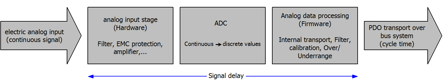
This process involves several functional components, which act more or less strongly in every AI (analog input) module:
- the electrical input circuit
- the analog/digital conversion
- the digital further processing
- the final provision of the process and diagnostic data for collection at the fieldbus (EtherCAT, K‑bus, etc.)
Two aspects are crucial from a user perspective:
- “How often do I receive new values?”, i.e. a sampling rate in terms of speed with regard to the device/channel
- What delay does the (whole) AD conversion of the device/channel cause?
I.e. the hardware and firmware components in its entirety. For technological reasons, the signal characteristics must be taken into account when determining this information: the run times through the system differ, depending on the signal frequency.
This is the “external” view of the “Beckhoff AI channel” system – internally the signal delay in particular is composed of different components: hardware, amplifier, conversion itself, data transport and processing. Internally a higher sampling rate may be used (e.g. in the deltaSigma converters) than is offered “externally” from the user perspective. From a user perspective of the “Beckhoff AI channel” component this is usually irrelevant or is specified accordingly, if it is relevant for the function.
For Beckhoff AI devices the following specification parameters for the AI channel are available for the user from a temporal perspective:
1. Minimum conversion time [ms, µs]
This is the reciprocal value of the maximum sampling rate [sps, samples per second]:
Indicates how often the analog channel makes a newly detected process data value available for collection by the fieldbus. Whether the fieldbus (EtherCAT, K-bus) fetches the value with the same speed (i.e. synchronous), or more quickly (if the AI channel operates in slow FreeRun mode) or more slowly (e.g. with oversampling), is then a question of the fieldbus setting and which modes the AI device supports.
For EtherCAT devices the so-called toggle bit indicates (by toggling) for the diagnostic PDOs when a newly determined analog value is available.
Accordingly, a maximum conversion time, i.e. a smallest sampling rate supported by the AI device, can be specified.
Corresponds to IEC 61131-2, section 7.10.2 2, “Sampling repeat time”
2. Typical signal delay
Corresponds to IEC 61131-2, section 7.10.2 1, “Sampling duration”. From this perspective it includes all internal hardware and firmware components, but not “external” delay components from the fieldbus or the controller (TwinCAT).
This delay is particularly relevant for absolute time considerations, if AI channels also provide a time stamp that corresponds to the amplitude value – which can be assumed to match the physically prevailing amplitude value at the time.
Due to the frequency-dependent signal delay time, a dedicated value can only be specified for a given signal. The value also depends on potentially variable filter settings of the channel.
A typical characterization in the device documentation may be:
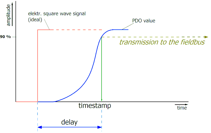
2.1 Signal delay (step response)
Keywords: Settling time
The square wave signal can be generated externally with a frequency generator (note impedance!)
The 90 % limit is used as detection threshold.
The signal delay [ms, µs] is then the time interval between the (ideal) electrical square wave signal and the time at which the analog process value has reached the 90 % amplitude.
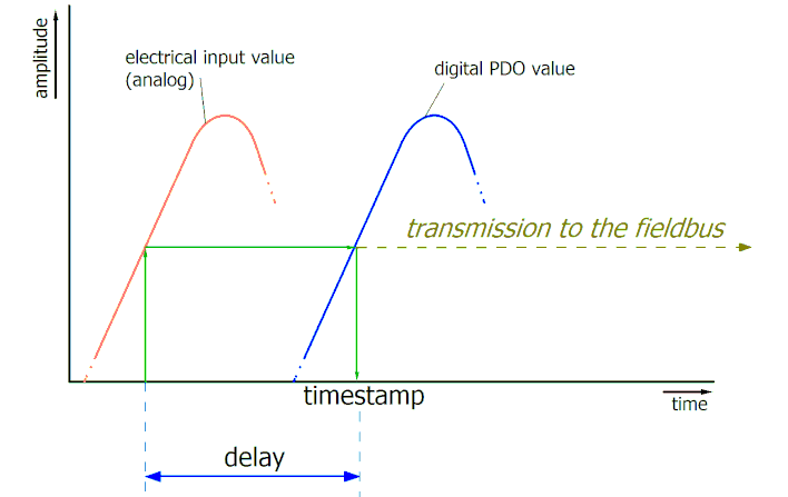
2.2 Signal delay (linear)
Keyword: Group delay
Describes the delay of a signal with constant frequency
A test signal can be generated externally with a frequency generator, e.g. as sawtooth or sine. A simultaneous square wave signal would be used as reference.
The signal delay [ms, µs] is then the interval between the applied electrical signal with a particular amplitude and the moment at which the analog process value reaches the same value.
A meaningful range must be selected for the test frequency, e.g. 1/20 of the maximum sampling rate.
3. Additional Information
May be provided in the specification, e.g.
- Actual sampling rate of the ADC (if different from the channel sampling rate)
- Time correction values for run times with different filter settings
- etc.