Structure of electrical strain gauges
A strain gauge consists of a carrier material (e.g. a stretchable plastic film) with an applied metal film from which a structure of deformable thin film electrical resistor is worked in very different geometrical forms, depending on the requirements.
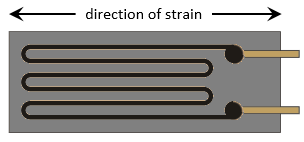
This utilizes a behavior whereby, for example in the case of strain, the length of a metallic resistance network increases and its diameter decreases, as a result of which its electrical resistance increases measurable:
ΔR/R = k · ε.
ε = Δl/l thereby corresponds to the relative elongation; the strain sensitivity is called the k‑factor. This also gives rise to the typical track layout of the conductive material within the strain gauge: the resistor track or course is laid in a meandering pattern in order to expose the longest possible length to the strain and to increase the selectivity of the force direction effect simultaneously.
Example:
The elongation ε = 0.1 % of a strain gauge with k‑factor 2 causes an increase in the resistance of 0.2 %. Typical resistive materials are constantan (k ≈ 2) or platinum tungsten (92PT, 8W with k ≈ 4). In the case of semiconductor strain gauges a silicon structure is glued to a carrier material. The conductivity is changed primarily by deformation of the crystal lattice (piezo‑resistive effect); k‑factors of up to 200 can be achieved.