Operation of inductive/capacitive loads on analog outputs
Analog outputs such as the EL40xx/41xx/EL47xx output terminals for standard signals (10 V/ 20 mA) or EL95xx adjustable power supply terminals are designed for ohmic loads. Since ideal ohmic resistive loads are difficult to achieve in practice, they can also drive inductive/capacitive loads within limits. Two effects must be taken into consideration when doing this:
- The current flowing through the inductor causes positive/negative voltage peaks depending on the rate of voltage rise.
- These must not exceed a level of 125 % of the max. nominal output voltage (unless otherwise specified in the respective device documentation).
Example: The EL4102 terminal specification states a max. output voltage of 10 V
→ max. ±12.5 V voltage peaks are permitted against analog GND. - Since the voltage/current source (i.e. the analog output) is controlled by the controller, the voltage/current rise can and must be deliberately selected to be slow enough to prevent unacceptably high voltages at the analog output.
- This must be checked by means of an oscilloscope during commissioning and an appropriate design must be selected to ensure that no overshoots occur at a later stage; if necessary, regular monitoring is required.
- A simulation is not sufficient.
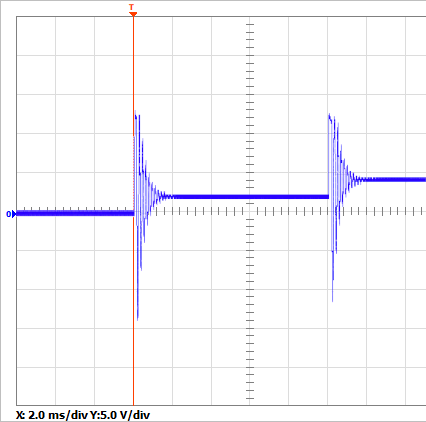
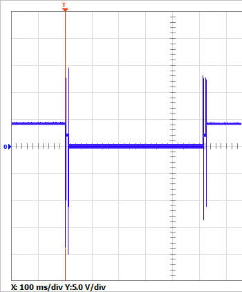
- Example with EL4112 terminal: Due to big output jumps (10,000 digits/cycle), impermissibly high overvoltages occur at an ohmic-inductive load at approx. 100 mH/ 320 Ω:
→ by distributing the rise over several stages, for example 1000 digits/cycle, the overvoltages are significantly reduced: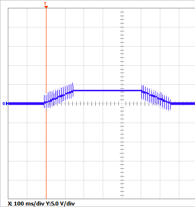
- oscillations may occur if the overall setup (with inductive and capacitive loads) results in a system capable of oscillating;
- an oscilloscope must be used to check that the inevitable oscillation decays again quickly (within a few milliseconds):