Example circuits for SW-side adjustable resistors
A first "common" and relatively simple circuit can be implemented using binary stepped resistors connected in series, each of which can be bridged with a switch: a pair of switches is used to bypass one resistor on the left side and one on the right side of the common node. Two switches from each switch block remain unused, as only two of each switch block (1:4 multiplexer group) are used. A 6-bit conversion would be the 1st example:
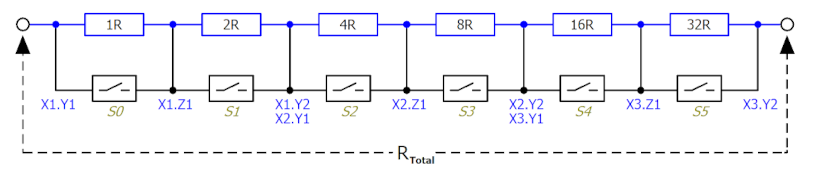 Fig.10: Example 1: binary stepped resistors connected in series
With the switch configuration S=#010010, for example, a resistance value of 45 Ω would result for R = 1 Ω if:
Rtotal = (S0neg ∙ 1 Ω + S1neg ∙ 2 Ω + S2neg ∙ 4 Ω + S3neg ∙ 8 Ω + S4neg ∙ 16 Ω + S5neg ∙ 32 Ω),
where S5 is the MSB. As a 1 = "switch closed" eliminates a resistance value and adds a value of 0 accordingly, the indices "neg" at S are given for "value negated".
In a 2nd example, all switches of a switch block are used. The resistors can be switched on and off in parallel:
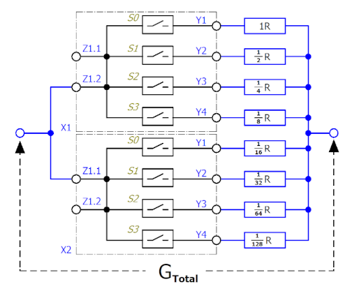 Fig.11: Example 2: binary stepped resistors connected parallel
Here, the calculation of the total resistance can be simplified somewhat with the help of the conductance: the MSB S7 adds the highest conductance 128 S for 1 = "switch closed", there is no negation. Overall, it behaves like a series connection:
Gtotal = (S0 ∙ 1 S + S1 ∙ 2 S + S2 ∙ 4 S + S3 ∙ 8 S + S4 ∙ 16 S + S5 ∙ 32 S + S6 ∙ 64 S + S7 ∙ 128 S)
As can be seen from the reciprocal value formation for Rtotal = (Gtotal)-1, in contrast to the series connection from the first example, a hyperbolic curve is present here. In the series connection from example 1, however, there is a linear relationship for each switch value to the resistance value. A combination of series and parallel connection in the 3rd example can transform the hyperbolic curve into a linear curve:
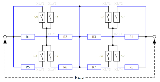 Fig.12: Example 3: binary stepped resistors connected in series and parallel
It can be seen that there are again redundant switch position combinations here, as S4, for example, has no effect if S0 is closed and so on. On the other hand, this circuit provides a linear curve, at least for (ideal) binary stepped resistance values. It is intended that the resistors R5 to R8 in sequence have the same values as R1 to R4 in sequence. E.g. when defining the values:
R1 = R5 = 2 Ω, R2 = R6 = 4 Ω, R3 = R7 = 8 Ω and R4 = R8 = 16 Ω
resistors from 0...30 Ω can be switched in one-ohm steps.
It makes sense to determine all the different total resistance values for each switch combination for all such circuits using a script. A practicable approach for example 3 in ST (TwinCAT 3.1) is given here in advance:
based on a function for calculating two resistors connected in parallel:
FUNCTION F_RG_PAR : LREAL
VAR_INPUT
   nR1, nR2 : LREAL;
END_VAR
// total resistance calculation of two parallel resistors
// special cases, if one resistor is zero the other will be returned
F_RG_PAR := SEL((nR1=0), SEL((nR2=0), ((nR1 * nR2)/(nR1 + nR2)), nR1), nR2);and a further function for calculating the total resistance:
FUNCTION F_RG_R_SIMU : LREAL
VAR_INPUT
   paR : POINTER TO ARRAY[1..16] OF LREAL;
   nS : UINT;
END_VAR
VAR
   nI : BYTE;
END_VAR
// total resistance calculation by nS: S0=bit0, S15=bit15
// (for 2 x 8 resistances using S8..S11 for S4..S7)
F_RG_R_SIMU := 0;
FOR nI := 0 TO 7 DO
F_RG_R_SIMU := F_RG_R_SIMU
+ SEL(((SHR(nS, nI) AND 1) = 1), F_RG_PAR(paR^[nI+1],
SEL(((SHR(nS, (nI+8)) AND 1) = 1), 0, paR^[nI+9])), 0);
END_FORthe following code can be used to calculate all total resistance values for given resistances from the circuit in example 3:
PROGRAM MAIN
VAR CONSTANT
   n8Bit             : UDINT := 255;
   //n16Bit          : UDINT := 65535;
END_VAR
VAR
   bStart            : BOOL := FALSE;
   bUse_E96          : BOOL := FALSE;
   // Array with resistor values 2 x 2, 2 x 4 and 2 x 8 circuit
   aR_List_bin       : ARRAY[1..16] OF LREAL := [
                         2, 4, 8, 16, 32, 64, 128, 256,
                         2 ,4 ,8 ,16 ,32 ,64 ,128 ,256
                         ];// Ideal/theoretical values
   aR_List_E96       : ARRAY[1..16] OF LREAL :=[
                         2, 4.02, 8.06, 16.16, 32.39, 63.4, 130.19, 261.02,
                         2, 4.02, 8.06, 16.16, 32.39, 63.4, 130.19, 261.02
                         ];
   aS_List           : ARRAY[0..n8Bit] OF UINT; // array size with max number of switch combinations for 2 x 4 circuit
   rValue            : ARRAY[0..n8Bit] OF LREAL; // array size with max number of total resistor values for 2 x 4 circuit
   nI, nJ, nMaxComb  : UDINT;
   nState            : BYTE := 0;
END_VAR
// execution part
CASE nState OF 0:
// create switch combinations:
// 1 = switch closed
IF bStart THEN
bStart := FALSE;
// use switches for circuit with 8 resistors
// S0..S3 and S8..S11
FOR nJ := 0 TO 15 DO
FOR nI := 0 TO 15 DO
aS_List[nI+16*nJ] := UDINT_TO_WORD(16#F0 OR (nI OR SHL(nJ, 8)));
// - unused switch combinations 0xXXF0, (S4..S7) must be closed
//(S12..S15 don't care)
END_FOR
END_FOR
// (for loops should be nState numbers when task cycle time not enough)
nMaxComb := n8Bit;
nI := 0;
nState := nState + 10;
END_IF
10:
// calculate total resistor values:
IF bUse_E96 THEN
rValue[nI] := F_RG_R_SIMU(ADR(aR_List_E96), aS_List[nI]);
ELSE
rValue[nI] := F_RG_R_SIMU(ADR(aR_List_bin), aS_List[nI]);
END_IF
IF(nI = nMaxComb) THEN
nState := 0;
END_IF
nI := nI + 1;
END_CASENote: when using these circuits, the on-resistance specified for the terminal used must be taken into account for the total resistance in the technical data, among other things!
Download tpzip file.