EL125x - Functioning
General features
The EL1252, EL1254 provides not only the input level, but also the last time stamp at which a channel underwent a rising or falling edge. The status byte for each channel provides information about changes in the latch processes.
 | Calibration The time delay between the physically real edge of the signal voltage at the terminal input and the time stamp in the EtherCAT slave controller (ESC) is kept below 1 µs by the optimized electronics, but is not indefinitely short. If the user has a particular need for precision, calibration must be carried out, and the precise time delay measured in accordance with the environmental conditions. |
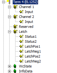
The terminal provides the following information for each channel (see Fig. TwinCAT tree, EL1252):
 Fig.149: TwinCAT tree, EL1252
- Status1/Status2
Depending on the terminal and setting in SingleEvent-Mode changes in the state of the channel in each of the status bytes Status1/Status2 are displayed in the bits 0.1and 2. The bits 3 to 7 are reserved and not recommended for evaluation.
Status Byte
EL1252 | 0 | 0->1 | 1 | 1->0 |
ContinuousMode (default) | 0 (b#00000000) | 0 (b#00000000) | 0 (b#00000000) | 0 (b#00000000) |
SingleEventMode | 0 (b#00000000) | 1 (b#00000001) | 1 (b#00000001) | 2 (b#00000010) |
|
|
|
|
|
EL1254 | 0 | 0->1 | 1 | 1->0 |
ContinuousMode (default) | 0 (b#00000000) | 4 (b#00000100) | 4 (b#00000100) | 0 (b#00000000) |
SingleEventMode | 0 (b#00000000) | 5 (b#00000101) | 4 (b#00000100) | 0 (b#00000000) |
- In SingleEventMode changes 0 -> 1/1 -> 0 are displayed for only one EtherCAT cycle, because reading the time LatchPosY/LatchNegY also resets the displayed changes.
- LatchPos1/LatchPos2
The time of the first/last rising signal edge (in the period of time between the most recent fieldbus cycle and the current read of the terminal by an EtherCAT frame) - LatchNeg1/LatchNeg2
The time of the first/last falling signal edge (in the period of time between the most recent fieldbus cycle and the current read of the terminal by an EtherCAT frame) - Channel 1 Input / Channel 2 Input
Input level 0 or 1
The times of the edges are made available in the form of 64-bit times, i.e. as 8 bytes of process data based on the Distributed Clock of the terminal.
They are constructed as follows: LatchPosXXXY (XXX: POS/NEG, rising or falling edge; Y: channel, 1 or 2).
 | Temporal consistency of the input data The input data of the EL1252, EL1254 can be functionally divided into two groups. This is also visible from their storage location in the ESC registers: The two data blocks are updated at different “speeds” - whilst the input data is read in and made available upon the arrival of the Ethernet frame at the EtherCAT slave, the DC latch times can still be updated during the processing of the datagram on account of the external latch event. Therefore, the latch times can still change up until a few ns before being read into the Ethernet frame - this ensures that it is really the latest possible status of the inputs that is mapped into the frame. |