Cycle time of 250 μs
Note that a cycle time of 250 μs on a CX7293 represents an extreme optimum and all boundary conditions must be right. Furthermore, a cycle time of 250 μs only makes sense if the inputs and outputs are correspondingly fast.
The CX7293 has different interfaces, including, for example, the K-bus. The K-bus can achieve perhaps 1 ms under optimal conditions and is therefore unsuitable for cycle times of 250 μs. The E-bus (EtherCAT) is much faster, but the structure of an EtherCAT frame and the merging of the data into an EtherCAT frame is much more complex, so that only 1 ms is possible here as well.
Of course, EtherCAT can be operated with other Industrial PCs under 100 μs. However, these are usually equipped with more powerful CPUs and may use a DMA controller for EtherCAT processing. That is not the case with the CX7293, however, so the CPU power and the interfaces to EtherCAT are the limiting factors. Of course, the CX7293 as a small controller was not developed for high-speed applications and, due to its cost-efficiency, should not be compared to more powerful Industrial PCs.
Setting a cycle time of 250 μs
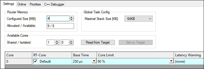
A cycle time of 250 μs is possible on a CX7293 if the boundary conditions are right. The CX7293 is helped by the multifunction I/Os, which are connected to the CPU via a fast IO connection. The connection is kept very lean and has a correspondingly good data throughput. It is possible to reach the 250 μs with the help of the multifunction I/Os. Of course, the PLC program may contain only very little code and the core limit must be set to 90%, which in turn results in the described disadvantages (see: Real-time and CPU load).

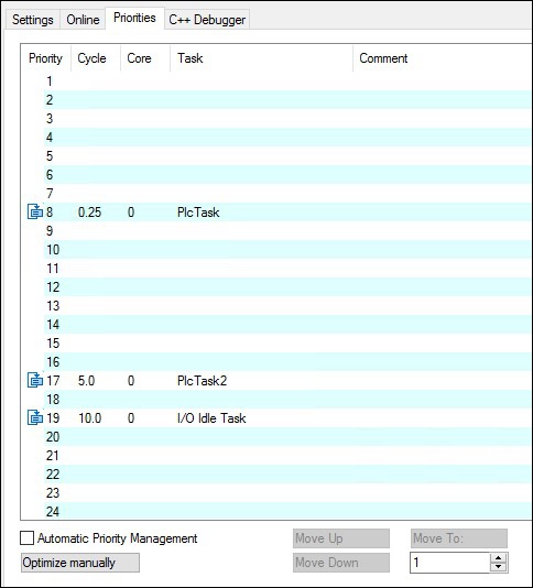
In addition, you should set the priority of the task so that the 250 μs task has the highest priority in the system.

If you now allow a digital output of the CX7028 interface to toggle, for example with Out_01:=not Out_01 in the 250 μs task, the task is output at a frequency of 2 kHz. In order for the output to be optimally fast, this output should have a load. Only wire the output with a digital input; as a result, the load is very small and the switch-off behavior of the driver is relatively slow. Slow here means in relation to the 250 μs task time. It makes a difference whether the output requires 50 μs or 100 μs to switch off. If you now wish to measure the response time, i.e. the time it takes for the CX7293 to react to an input, the following background is important:
From a cycle time of 1 ms or greater, an optimal cycle is operated, i.e. the inputs of the CX7028 interface are read by the processor of the CX7028 interface about 20% before the new task cycle. If the task time is faster than 1 ms, the time is not sufficient for the optimized response time. In this case the inputs are read with the task cycle. As a result, a task time of 500 μs achieves the same response time as a task time of 1 ms. With a task time of less than 1 ms, the update needs four task cycles for a cycle. With 1 ms or slower it needs two task cycles. This should make you aware that it is not always the shortening of the cycle time that shortens the reaction time, but also the internal process, which plays a decisive role in the reading of the data.
Here is a sample, so that you can reproduce this behavior yourself and see and measure the differences:
- Connect the +24 V Up and 0 V Up power supply to power the multifunction I/Os.
- Connect output 1 to input 1 to toggle the output as described.
- Connect output 2 to input 2.
- Set the core limit to 90%, the base time to 250 μs, the priority of the fast task to the highest priority, and the idle task to 10 ms.
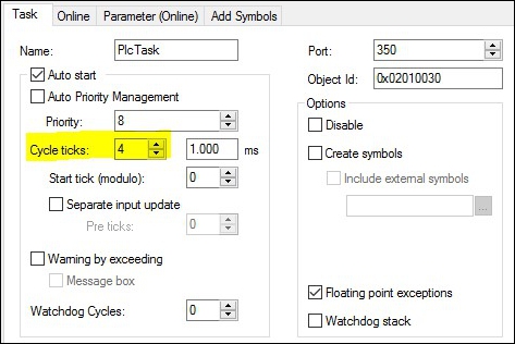
The inputs have only a minimal filter time and are therefore well suited for the measurement. A load on the output is not necessary in this case. For the following samples, we always leave the base time at 250 μs and only increase the number of cycle ticks in order to set the corresponding task time.

Sample program
PROGRAM MAIN
VAR
    bOut_1 AT %Q*:BOOL; (*toggle Output link to digital Output pin 7*)
    bOut_2 AT %Q*:BOOL; (*reaction time link to digital Output pin 14*)

    bIn_1 AT %I*: BOOL; (*toggle Output link to digital Input pin 2*)
    bIn_2 AT %I*: BOOL; (*reaction time link to digital Input pin 10*)

    fbTimer : TON;
    fbflanke1 : R_TRIG;
    fbflanke2 : R_TRIG;

    cnt1: INT; (*toggle Output*)
    cnt1_M: INT; (*toggle Output*)

    cnt2: INT; (*reaction time*)
    cnt2_M: INT; (*reaction time*)
END_VAR


PROGRAM MAIN
bOut_1:= NOT bOut_1; (*toggle Output*)
bOut_2:= NOT bIn_2; (*reaction time*)

fbflanke1(CLK:=bIn_1);
IF fbflanke1.Q THEN
    cnt1:=cnt1+1; (*toggle Output*)
END_IF

fbflanke2(CLK:=bIn_2);
IF fbflanke2.Q THEN
    cnt2:=cnt2+1; (*reaction time*)
END_IF

fbTimer(PT:=T#1S,in:=NOT fbTimer.Q);

IF fbTimer.Q THEN
    cnt2_M:=cnt2; (*reaction time*)
    cnt1_M:=cnt1; (*toggle Output*)
    cnt1:=0;
    cnt2:=0;
END_IF
The toggling of the output results in a frequency of 2 kHz – 250 μs On, 250 μs Off – i.e. a period duration of 500 μs. When measuring the positive edge, this is 2000 edge changes in one second.
 Fig.43: Measurement at a task time of 250 μs.
In the case of the response time, it is 500 changes in one second, as the optimized access to the inputs does not apply here.
 Fig.44: Measurement at a task time of 500 μs.
As expected, the values are only half as large with a task time that is twice as long.
 Fig.45: Measurement at a task time of 1 ms.
With a task time of 1 ms, you can clearly see that the optimized mode actually helps to reduce the response time. While the toggle change has halved again, i.e. it is now still 500 Hz with a task time of 1 ms, the value for the response time has remained the same.