Objects and Data
Device type
Index | Subindex | Name | Type | Attribute | Mapping | Default value | Meaning |
|---|---|---|---|---|---|---|---|
0x1000 | 0 | Device Type | Unsigned32 | ro | N | 0x00000000 | Statement of device type |
The 32-bit value is divided into two 16-bit fields:
MSB | LSB |
|---|---|
Additional Information | Device profile number |
0000 0000 0000 wxyz | 0x191 (401dec) |
The additional information contains data related to the signal type of the I/O device:
z=1 signifies digital inputs,
y=1 signifies digital outputs,
x=1 signifies analog inputs,
w=1 signifies analog outputs.
A BK5120 with digital and analog inputs, but with no outputs, thus returns 0x00 05 01 91.
Special terminals (such as serial interfaces, PWM outputs, incremental encoder inputs) are not considered. A Coupler that, e.g. only has KL6001 serial interface terminals plugged in, thus returns 0x00 00 01 91.
The device type supplies only a rough classification of the device. The terminal identifier register of the Bus Coupler can be read for detailed identification of the Bus Couplers and the attached terminals (for details see Register communication index 0x4500).
Error register
Index | Subindex | Name | Type | Attribute | Mapping | Default value | Meaning |
|---|---|---|---|---|---|---|---|
0x1001 | 0 | Error Register | Unsigned8 | ro | N | 0x00 | Error register |
The 8-bit value is coded as follows:
Bit 7 | Bit 6 | Bit 5 | Bit 4 | Bit 3 | Bit 2 | Bit 1 | Bit 0 |
|---|---|---|---|---|---|---|---|
ManSpec. | reserved | reserved | Comm. | reserved | reserved | reserved | Generic |
ManSpec. Manufacturer-specific error, specified more precisely in object 0x1003.
Comm.: Communication error (CAN overrun)
Generic: An error that is not more precisely specified has occurred (the flag is set at every error message)
Error memory
Index | Subindex | Name | Type | Attribute | Mapping | Default value | Meaning |
|---|---|---|---|---|---|---|---|
0x1003 | 0x00 | Predefined error field (error memory) | Unsigned8 | rw | N | 0x00 | Object 1003h contains a description of the error that has occurred in the device - subindex 0 has the number of error states stored. |
1 | Actual error | Unsigned32 | ro | N | none | Last error state to have occurred | |
... | ... | ... | -- | ... | ... | ... | |
10 | Standard error field | Unsigned32 | ro | N | none | A maximum of 10 error states are stored. |
The 32 bit value in the error memory is divided into two 16 bit fields:
MSB | LSB |
|---|---|
Additional Code | Error Code |
The additional code contains the error trigger (see emergency object) and thereby a detailed error description.
New errors are always saved at subindex 1, all the other subindices being appropriately incremented. The whole error memory is cleared by writing a 0 to subindex 0.
If there has not been an error since power up, then object 0x1003 only consists of subindex 0 with a 0 entered into it. The error memory is cleared by a reset or a power cycle.
As is usual in CANopen, the LSB is transferred first, followed by the MSB.
Sync Identifier
Index | Subindex | Name | Type | Attribute | Mapping | Default value | Meaning |
|---|---|---|---|---|---|---|---|
0x1005 | 0 | COB-ID Sync Message | Unsigned32 | rw | N | 0x80000080 | Identifier of the SYNC message |
The bottom 11 bits of the 32-bit value contain the identifier (0x80=128 dec). Bit 30 indicates whether the device sends the SYNC telegram (1) or not (0). The CANopen I/O devices receive the SYNC telegram, and accordingly bit 30=0. For reasons of backwards compatibility, bit 31 has no significance.
Sync Interval
Index | Subindex | Name | Type | Attribute | Mapping | Default value | Meaning |
|---|---|---|---|---|---|---|---|
0x1006 | 0 | Communication cycle period | Unsigned32 | rw | N | 0x00000000 | Length of the SYNC interval in µs. |
If a value other than zero is entered here, the bus node will go into the error state if, during synchronous PDO operation, no SYNC telegram is received within the watchdog time. The watchdog time corresponds here to 1,5 times the communication cycle period that has been set - the planned SYNC interval can therefore be entered.
The I/O update is carried out at the Beckhoff CANopen bus nodes immediately after reception of the SYNC telegram, provided the following conditions are satisfied:
- Firmware status C0 or above (CANopen Version 4.01 or higher).
- All PDOs that have data are set to synchronous communication (0...240).
- Sync interval has been entered in object 0x1006 and (sync interval x lowest PDO transmission type) is less than 90ms.
The modules are then synchronized throughout.
Device name
Index | Subindex | Name | Type | Attribute | Mapping | Default value | Meaning |
|---|---|---|---|---|---|---|---|
0x1008 | 0 | Manufacturer Device Name | Visible String | ro | N | BK51x0, LC5100, | Device name of the bus node |
Since the returned value is longer than 4 bytes, the segmented SDO protocol is used for transmission.
Hardware-Version
Index | Subindex | Name | Type | Attribute | Mapping | Default value | Meaning |
|---|---|---|---|---|---|---|---|
0x1009 | 0 | Manufacturer Hardware-Version | Visible String | ro | N | - | Hardware version number of the bus node |
Since the returned value is longer than 4 bytes, the segmented SDO protocol is used for transmission.
Software version
Index | Subindex | Name | Type | Attribute | Mapping | Default value | Meaning |
|---|---|---|---|---|---|---|---|
0x100A | 0 | Manufacturer Software-Version | Visible String | ro | N | - | Software version number of the bus node |
Since the returned value is longer than 4 bytes, the segmented SDO protocol is used for transmission.
Node number
Index | Subindex | Name | Type | Attribute | Mapping | Default value | Meaning |
|---|---|---|---|---|---|---|---|
0x100B | 0 | Node-ID | Unsigned32 | ro | N | none | Set node number |
The node number is supported for reasons of compatibility.
Guard Time
Index | Subindex | Name | Type | Attribute | Mapping | Default value | Meaning |
|---|---|---|---|---|---|---|---|
0x100C | 0 | Guard Time [ms] | Unsigned16 | rw | N | 0 | Interval between two guard telegrams. Is set by the NMT master or configuration tool. |
Life Time Factor
Index | Subindex | Name | Type | Attribute | Mapping | Default value | Meaning |
|---|---|---|---|---|---|---|---|
0x100D | 0 | Life Time Factor | Unsigned8 | rw | N | 0 | Life time factor x guard time = life time (watchdog for life guarding) |
If a guarding telegram is not received within the life time, the node enters the error state. If the life time factor and/or guard time = 0, the node does not carry out any life guarding, but can itself be monitored by the master (node guarding).
Guarding Identifier
Index | Subindex | Name | Type | Attribute | Mapping | Default value | Meaning |
|---|---|---|---|---|---|---|---|
0x100 E | 0 | COB-ID guarding protocol | Unsigned32 | ro | N | 0x000007xy, xy = NodeID | Identifier of the guarding protocol |
The guarding identifier is supported for reasons of compatibility. Changing the guarding identifier has no longer been permitted since version 4 of CANopen.
Save parameters
Index | Subindex | Name | Type | Attribute | Mapping | Default value | Meaning |
|---|---|---|---|---|---|---|---|
0x1010 | 0 | Store Parameter | Unsigned8 | ro | N | 1 | Number of store options |
1 | store all parameters | Unsigned32 | rw | N | 1 | Stores all (storable) parameters |
By writing the string save in ASCII code (hexadecimal 0x65766173) to subindex 1, the current parameters are placed into non-volatile storage. (The byte sequence on the bus including the SDO protocol: 0x23 0x10 0x10 0x01 0x73 0x61 0x76 0x65).
The storage process takes about 3 seconds, and is confirmed, if successful, by the corresponding TxSDO (0x60 in the first byte). Since the Bus Coupler is unable to send or receive any CAN telegrams during the storage process, saving is only possible when the node is in the pre-operational state. It is recommended that the entire network is placed into the pre-operational state before such storage. This avoids a buffer overflow.
Data saved includes:
- The terminals currently inserted (the number of each terminal category)
- All PDO parameters (identifier, transmission type, inhibit time, mapping).
 | Valid identifiers The stored identifiers apply afterwards, not the default identifiers derived from the node addresses. Changes to the DIP switch setting no longer affects the PDOs! |
- All SYNC parameters
- All guarding parameters
- Limit values, delta values and interrupt enables for analog inputs
Parameters directly stored in the terminals by way of register communication are immediately stored there in non-volatile form.
Load default values
Index | Subindex | Name | Type | Attribute | Mapping | Default value | Meaning |
|---|---|---|---|---|---|---|---|
0x1011 | 0 | Restore Parameter | Unsigned8 | ro | N | 4 | Number of reset options |
1 | Restore all parameters | Unsigned32 | rw | N | 1 | Resets all parameters to their default values | |
4 | Set manufacturer Defaults | Unsigned32 | rw | N | 1 | Resets all coupler parameters to manufacturer’s settings (including registers) |
Writing the string load in ASCII code (hexadecimal 0x64616F6C) into subindex 1 resets all parameters to default values (as initially supplied) at the next boot (reset).
(The byte sequence on the bus including the SDO protocol: 0x23 0x11 0x10 0x01 0x6C 0x6F 0x61 0x64).
This makes the default identifiers for the PDOs active again.
Emergency Identifier
Index | Subindex | Name | Type | Attribute | Mapping | Default value | Meaning |
|---|---|---|---|---|---|---|---|
0x1014 | 0 | COB-ID Emergency | Unsigned32 | rw | N | 0x00000080, + NodeID | Identifier of the emergency telegram |
The bottom 11 bits of the 32-bit value contain the identifier (0x80=128 dec). The MSBit can be used to set whether the device sends (1) the emergency telegram or not (0).
Alternatively, the bus node's diagnostic function can also be switched off using the Device diagnostics bit in the K-bus configuration (see object 0x4500).
Consumer Heartbeat Time
Index | Subindex | Name | Type | Attribute | Mapping | Default value | Meaning |
|---|---|---|---|---|---|---|---|
0x1016 | 0 | Number of items | Unsigned8 | ro | N | 2 | The consumer heartbeat time describes the expected heartbeat cycle time and the node ID of the monitored node |
1 | Consumer Heartbeat Time | Unsigned32 | rw | N | 0 | Watchdog time in ms and node ID of the monitored node |
The 32-bit value is used as follows:
MSB | LSB | |
|---|---|---|
Bit 31...24 | Bit 23...16 | Bit 15...0 |
Reserved (0) | Node-ID (Unsigned8) | heartbeat time in ms (Unsigned16) |
The monitored identifier can be obtained from the node ID by means of the default identifier allocation: Guard-ID = 0x700 + Node-ID.
As is usual in CANopen, the LSB is transferred first, followed by the MSB.
Producer Heartbeat Time
Index | Subindex | Name | Type | Attribute | Mapping | Default value | Meaning |
|---|---|---|---|---|---|---|---|
0x1017 | 0 | Producer Heartbeat Time | Unsigned16 | rw | N | 0 | Time interval in ms between two transmitted heartbeat telegrams |
Device identifier (identity object)
Index | Subindex | Name | Type | Attribute | Mapping | Default value | Meaning |
|---|---|---|---|---|---|---|---|
0x1018 | 0 | Identity Object: Number of items | Unsigned8 | ro | N | 4 | The identity object contains general information about the type and version of the device. |
1 | Vendor ID | Unsigned32 | ro | N | 0x00000002 | Manufacturer identifier. Beckhoff has vendor ID 2 | |
2 | Product Code | Unsigned32 | ro | N | Depends on the product | Device identifier | |
3 | Revision Number | Unsigned32 | ro | N | - | Version number | |
4 | Serial Number | Unsigned32 | ro | N | - | Date of manufacture |
Product | Product Code |
|---|---|
BK5120 | 0x11400 |
BK5110 | 0x113F6 |
LC5100 | 0x113EC |
IPwxyz-B510 | 0x2wxyz |
IL2301-B510 | 0x2008FD |
Server SDO parameters
Index | Subindex | Name | Type | Attribute | Mapping | Default value | Meaning |
|---|---|---|---|---|---|---|---|
0x1200 | 0 | Number of items | Unsigned8 | ro | N | 2 | Communication parameters of the server SDO. Subindex 0: Number of following parameters |
1 | COB-ID Client ->Server | Unsigned32 | ro | N | 0x000006xy, xy=Node-ID | COB-ID RxSDO (Client -> Server) | |
2 | COB-ID Server ->Client | Unsigned32 | ro | N | 0x00000580 + Node-ID | COB-ID TxSDO (Client -> Server) |
This is contained in the object directory for reasons of backwards compatibility.
Communication parameter 1st RxPDO
Index | Subindex | Name | Type | Attribute | Mapping | Default value | Meaning |
|---|---|---|---|---|---|---|---|
0x1400 | 0 | Number of items | Unsigned8 | ro | N | 5 | Communication parameters for the first receive PDO. Subindex 0: Number of following parameters |
1 | COB-ID | Unsigned32 | rw | N | 0x000002xy, xy=Node-ID | COB-ID (Communication Object Identifier) RxPDO1 | |
2 | Transmission Type | Unsigned8 | rw | N | 255 | Transmission type of the PDO | |
3 | Inhibit Time | Unsigned16 | rw | N | 0 | Present for reasons of backwards compatibility, but not used in the RxPDO. | |
4 | CMS Priority Group | Unsigned8 | rw | N | - | Present for reasons of backwards compatibility, but not used. | |
5 | Event Timer | Unsigned16 | rw | N | 0 | Event-Timer. Watchdog time defined for monitoring reception of the PDO. |
Subindex 1 (COB-ID): The bottom 11 bits of the 32 bit value (bits 0-10) contain the CAN identifier. The MSB (bit 31) indicates whether the PDO exists currently (0) or not (1). Bit 30 indicates whether an RTR access to this PDO is permissible (0) or not (1). Changing the identifier (bits 0-10) is not allowed while the object exists (bit 31=0). Subindex 2 contains the transmission type (see introduction to PDOs).
Communication parameter 2nd RxPDO
Index | Subindex | Name | Type | Attribute | Mapping | Default value | Meaning |
|---|---|---|---|---|---|---|---|
0x1401 | 0 | Number of items | Unsigned8 | ro | N | 5 | Communication parameter for the second receive PDO. |
1 | COB-ID | Unsigned32 | rw | N | 0x000003xy, xy=Node-ID | COB-ID (Communication Object Identifier) RxPDO2 | |
2 | Transmission Type | Unsigned8 | rw | N | 255 | Transmission type of the PDO | |
3 | Inhibit Time | Unsigned16 | rw | N | 0 | Present for reasons of backwards compatibility, but not used in the RxPDO. | |
4 | CMS Priority Group | Unsigned8 | rw | N | - | Present for reasons of backwards compatibility, but not used. | |
5 | Event Timer | Unsigned16 | rw | N | 0 | Event-Timer. Watchdog time defined for monitoring reception of the PDO. |
Communication parameter 3rd RxPDO
Index | Subindex | Name | Type | Attribute | Mapping | Default value | Meaning |
|---|---|---|---|---|---|---|---|
0x1402 | 0 | Number of items | Unsigned8 | ro | N | 5 | Communication parameter for the third receive PDO. |
1 | COB-ID | Unsigned32 | rw | N | 0x000004xy, xy=Node-ID | COB-ID (Communication Object Identifier) RxPDO3 | |
2 | Transmission Type | Unsigned8 | rw | N | 255 | Transmission type of the PDO | |
3 | Inhibit Time | Unsigned16 | rw | N | 0 | Present for reasons of backwards compatibility, but not used in the RxPDO. | |
4 | CMS Priority Group | Unsigned8 | rw | N | - | Present for reasons of backwards compatibility, but not used. | |
5 | Event Timer | Unsigned16 | rw | N | 0 | Event-Timer. Watchdog time defined for monitoring reception of the PDO. |
Communication parameter 4th RxPDO
Index | Subindex | Name | Type | Attribute | Mapping | Default value | Meaning |
|---|---|---|---|---|---|---|---|
0x1403 | 0 | Number of items | Unsigned8 | ro | N | 5 | Communication parameters for the fourth receive PDO. |
1 | COB-ID | Unsigned32 | rw | N | 0x000005xy, xy=Node-ID | COB-ID (Communication Object Identifier) RxPDO4 | |
2 | Transmission Type | Unsigned8 | rw | N | 255 | Transmission type of the PDO | |
3 | Inhibit Time | Unsigned16 | rw | N | 0 | Present for reasons of backwards compatibility, but not used in the RxPDO. | |
4 | CMS Priority Group | Unsigned8 | rw | N | - | Present for reasons of backwards compatibility, but not used. | |
5 | Event Timer | Unsigned16 | rw | N | 0 | Event-Timer. Watchdog time defined for monitoring reception of the PDO. |
Communication parameters 5th-16th RxPDO
Index | Subindex | Name | Type | Attribute | Mapping | Default value | Meaning |
|---|---|---|---|---|---|---|---|
0x1404 - 0x140F (depending on the device type) | 0 | Number of items | Unsigned8 | ro | N | 5 | Communication parameter for the 5th to 16th receive PDOs. |
1 | COB-ID | Unsigned32 | rw | N | 0x8000000 | COB-ID (Communication Object Identifier) RxPDO5...16 | |
2 | Transmission Type | Unsigned8 | rw | N | 255 | Transmission type of the PDO | |
3 | Inhibit Time | Unsigned16 | rw | N | 0 | Present for reasons of backwards compatibility, but not used in the RxPDO. | |
4 | CMS Priority Group | Unsigned8 | rw | N | - | Present for reasons of backwards compatibility, but not used. | |
5 | Event Timer | Unsigned16 | rw | N | 0 | Event-Timer. Watchdog time defined for monitoring reception of the PDO. |
The number of RxPDOs for each bus node type can be found in the technical data.
Parameter / mapping RxPDO
Index | Subindex | Name | Type | Attribute | Mapping | Default value | Meaning |
|---|---|---|---|---|---|---|---|
0x1600 | 0 | Number of items | Unsigned8 | rw | N | Depending on type and fittings | Mapping parameter of the first receive PDO; subindex 0: number of mapped objects. |
1 | 1st mapped object | Unsigned32 | rw | N | 0x62000108 | 1st mapped application object (2 bytes index, 1 byte subindex, 1 byte bit width) | |
2 | 2nd mapped object | Unsigned32 | rw | N | 0x62000208 | 2nd mapped application object (2 bytes index, 1 byte subindex, 1 byte bit width) | |
... | ... | ... | ... | ... | ... | ... | |
8 | 8th mapped object | Unsigned32 | rw | N | 0x62000808 | 8th mapped application object (2 bytes index, 1 byte subindex, 1 byte bit width) |
The first receive PDO (RxPDO1) is provided by default for digital output data. Depending on the number of outputs inserted, the necessary length of the PDO is automatically determined, and the corresponding objects are mapped. Since the digital outputs are organized in bytes, the length of the PDO in bytes can be found directly at subindex 0.
Changes to the mapping
The following sequence must be observed in order to change the mapping (specified as from CANopen, version 4):
- Delete PDO (set bit 31 in the identifier entry (subindex 1) of the communication parameters to 1)
- Deactivate mapping (set subindex 0 of the mapping entry to 0)
- Change mapping entries (subindices 1...8)
- Activate mapping (set subindex 0 of the mapping entry to the correct number of mapped objects)
- Create PDO (set bit 31 in the identifier entry (subindex 1) of the communication parameters to 0)
Mapping parameter 2nd RxPDO
Index | Subindex | Name | Type | Attribute | Mapping | Default value | Meaning |
|---|---|---|---|---|---|---|---|
0x1601 | 0 | Number of items | Unsigned8 | rw | N | Depending on type and fittings | Mapping parameter of the second receive PDO; subindex 0: number of mapped objects. |
1 | 1st mapped object | Unsigned32 | rw | N | 0x64110110 | 1st mapped application object (2 bytes index, 1 byte subindex, 1 byte bit width) | |
2 | 2st mapped object | Unsigned32 | rw | N | 0x64110210 | 2nd mapped application object (2 bytes index, 1 byte subindex, 1 byte bit width) | |
... | ... | ... | ... | ... | ... | ... | |
8 | 8th mapped object | Unsigned32 | rw | N | 0x00000000 | 8th mapped application object (2 bytes index, 1 byte subindex, 1 byte bit width) |
The second receive PDO (RxPDO2) is provided by default for analog outputs. Depending on the number of outputs inserted, the necessary length of the PDO is automatically determined, and the corresponding objects are mapped. Since the analog outputs are organized in words, the length of the PDO in bytes can be found directly at subindex 0.
A specific sequence must be observed in order to change the mapping (see object index 0x1600).
Mapping-parameters 3rd - 16th RxPDO
Index | Subindex | Name | Type | Attribute | Mapping | Default value | Meaning |
|---|---|---|---|---|---|---|---|
0x1602- 0x160F (depending on the device type) | 0 | Number of items | Unsigned8 | rw | N | Depending on type and fittings | Mapping parameters for the 3rd to 16th receive PDOs; subindex 0: number of mapped objects. |
1 | 1st mapped object | Unsigned32 | rw | N | 0x00000000 (see text) | 1st mapped application object (2 bytes index, 1 byte subindex, 1 byte bit width) | |
2 | 2nd mapped object | Unsigned32 | rw | N | 0x00000000 (see text) | 2nd mapped application object (2 bytes index, 1 byte subindex, 1 byte bit width) | |
... | ... | ... | ... | ... | ... | ... | |
8 | 8th mapped object | Unsigned32 | rw | N | 0x00000000 (see text) | 8th mapped application object (2 bytes index, 1 byte subindex, 1 byte bit width) |
The 3rd to 16th receive PDOs (RxPDO3ff) are automatically given a default mapping by the bus node depending on the attached terminals (or depending on the extension modules). The procedure is described in the section on PDO Mapping.
A specific sequence must be observed in order to change the mapping (see object index 0x1600).
| Beckhoff Default Mapping DS401 V2 specifies analog input and/or output data as the default mapping for PDOs 3 and 4. This corresponds to Beckhoff's default mapping when less than 65 digital inputs or outputs are present. In order to ensure backwards compatibility, the Beckhoff default mapping is retained - the mapping behavior of the devices therefore corresponds to DS401 V1, where in all other respects they accord with DS401 V2. |
Communication parameter 1st TxPDO
Index | Subindex | Name | Type | Attribute | Mapping | Default value | Meaning |
|---|---|---|---|---|---|---|---|
0x1800 | 0 | Number of items | Unsigned8 | ro | N | 5 | Communication parameters for the first transmit PDO. Subindex 0: Number of following parameters |
1 | COB-ID | Unsigned32 | rw | N | 0x00000180 + Node-ID | COB-ID (Communication Object Identifier) TxPDO1 | |
2 | Transmission Type | Unsigned8 | rw | N | 255 | Transmission type of the PDO | |
3 | Inhibit Time | Unsigned16 | rw | N | 0 | Repetition delay [value x 100 µs] | |
4 | CMS Priority Group | Unsigned8 | rw | N | - | Present for reasons of backwards compatibility, but not used. | |
5 | Event Timer | Unsigned16 | rw | N | 0 | Event-Timer |
Subindex 1 (COB-ID): The bottom 11 bits of the 32 bit value (bits 0-10) contain the CAN identifier. The MSB (bit 31) indicates whether the PDO exists currently (0) or not (1). Bit 30 indicates whether an RTR access to this PDO is permissible (0) or not (1). Changing the identifier (bits 0-10) is not allowed while the object exists (bit 31=0). Subindex 2 contains the transmission type, subindex 3 the repetition delay between two PDOs of the same type, while subindex 5 contains the event timer. Subindex 4 is retained for reasons of compatibility, but is not used. (See also Introduction to PDOs.)
Communication parameter 2nd TxPDO
Index | Subindex | Name | Type | Attribute | Mapping | Default value | Meaning |
|---|---|---|---|---|---|---|---|
0x1801 | 0 | Number of items | Unsigned8 | ro | N | 5 | Communication parameters for the second transmit PDO. Subindex 0: Number of following parameters |
1 | COB-ID | Unsigned32 | rw | N | 0x00000280 + Node-ID | COB-ID (Communication Object Identifier) TxPDO1 | |
2 | Transmission Type | Unsigned8 | rw | N | 255 | Transmission type of the PDO | |
3 | Inhibit Time | Unsigned16 | rw | N | 0 | Repetition delay [value x 100 µs] | |
4 | CMS Priority Group | Unsigned8 | rw | N | - | Present for reasons of backwards compatibility, but not used. | |
5 | Event Timer | Unsigned16 | rw | N | 0 | Event-Timer |
The second transmit PDO is provided by default for analog inputs, and is configured for event-driven transmission (transmission type 255). Event-driven mode must first be activated (see object 0x6423), otherwise the inputs can only be interrogated (polled) by Remote Transmission Request (RTR).
Communication parameter 3rd TxPDO
Index | Subindex | Name | Type | Attribute | Mapping | Default value | Meaning |
|---|---|---|---|---|---|---|---|
0x1802 | 0 | Number of items | Unsigned8 | ro | N | 5 | Communication parameters for the third transmit PDO. Subindex 0: Number of following parameters |
1 | COB-ID | Unsigned32 | rw | N | 0x00000380 + Node-ID | COB-ID (Communication Object Identifier) TxPDO1 | |
2 | Transmission Type | Unsigned8 | rw | N | 255 | Transmission type of the PDO | |
3 | Inhibit Time | Unsigned16 | rw | N | 0 | Repetition delay [value x 100 µs] | |
4 | CMS Priority Group | Unsigned8 | rw | N | - | Present for reasons of backwards compatibility, but not used. | |
5 | Event Timer | Unsigned16 | rw | N | 0 | Event-Timer |
The third transmit PDO contains analog input data as a rule (see Mapping). It is configured for event-driven transmission (transmission type 255). Event-driven mode must first be activated (see object 0x6423), otherwise the inputs can only be interrogated (polled) by Remote Transmission Request (RTR).
Communication parameter 4th TxPDO
Index | Subindex | Name | Type | Attribute | Mapping | Default value | Meaning |
|---|---|---|---|---|---|---|---|
0x1803 | 0 | Number of items | Unsigned8 | ro | N | 5 | Communication parameters for the fourth transmit PDO. Subindex 0: Number of following parameters |
1 | COB-ID | Unsigned32 | rw | N | 0x00000480 + Node-ID | COB-ID (Communication Object Identifier) TxPDO1 | |
2 | Transmission Type | Unsigned8 | rw | N | 255 | Transmission type of the PDO | |
3 | Inhibit Time | Unsigned16 | rw | N | 0 | Repetition delay [value x 100 µs] | |
4 | CMS Priority Group | Unsigned8 | rw | N | - | Present for reasons of backwards compatibility, but not used. | |
5 | Event Timer | Unsigned16 | rw | N | 0 | Event-Timer |
The fourth transmit PDO contains analog input data as a rule (see Mapping). It is configured for event-driven transmission (transmission type 255). Event-driven mode must first be activated (see object 0x6423), otherwise the inputs can only be interrogated (polled) by Remote Transmission Request (RTR).
Communication parameters 5th - 16th RxPDO
Index | Subindex | Name | Type | Attribute | Mapping | Default value | Meaning |
|---|---|---|---|---|---|---|---|
0x1804- 0x180F (depending on the device type) | 0 | Number of items | Unsigned8 | ro | N | 5 | Communication parameters for the 5th - 16th transmit PDOs. Subindex 0: Number of following parameters |
1 | COB-ID | Unsigned32 | rw | N | 0x0000000 | COB-ID (Communication Object Identifier) TxPDO1 | |
2 | Transmission Type | Unsigned8 | rw | N | 255 | Transmission type of the PDO | |
3 | Inhibit Time | Unsigned16 | rw | N | 0 | Repetition delay [value x 100 µs] | |
4 | CMS Priority Group | Unsigned8 | rw | N | - | Present for reasons of backwards compatibility, but not used. | |
5 | Event Timer | Unsigned16 | rw | N | 0 | Event-Timer |
Mapping 1nd TxPDO
Index | Subindex | Name | Type | Attribute | Mapping | Default value | Meaning |
|---|---|---|---|---|---|---|---|
0x1A00 | 0 | Number of items | Unsigned8 | rw | N | Depending on type and fittings | Mapping parameter of the first transmit PDO; subindex 0: number of mapped objects. |
1 | 1st mapped object | Unsigned32 | rw | N | 0x60000108 | 1st mapped application object (2 bytes index, 1 byte subindex, 1 byte bit width) | |
2 | 2nd mapped object | Unsigned32 | rw | N | 0x60000208 | 2nd mapped application object (2 bytes index, 1 byte subindex, 1 byte bit width) | |
... | ... | ... | ... | ... | ... | ... | |
8 | 8th mapped object | Unsigned32 | rw | N | 0x60000808 | 8th mapped application object (2 bytes index, 1 byte subindex, 1 byte bit width) |
The first transmit PDO (TxPDO1) is provided by default for digital input data. Depending on the number of inputs inserted, the necessary length of the PDO is automatically determined, and the corresponding objects are mapped. Since the digital inputs are organized in bytes, the length of the PDO in bytes can be found directly at subindex 0.
A specific sequence must be observed in order to change the mapping (see object index 0x1600).
Mapping 2nd TxPDO
Index | Subindex | Name | Type | Attribute | Mapping | Default value | Meaning |
|---|---|---|---|---|---|---|---|
0x1A01 | 0 | Number of items | Unsigned8 | rw | N | Depending on type and fittings | Mapping parameter of the second transmit PDO; subindex 0: number of mapped objects. |
1 | 1st mapped object | Unsigned32 | rw | N | 0x64010110 | 1st mapped application object (2 bytes index, 1 byte subindex, 1 byte bit width) | |
2 | 2nd mapped object | Unsigned32 | rw | N | 0x64010210 | 2nd mapped application object (2 bytes index, 1 byte subindex, 1 byte bit width) | |
... | ... | ... | ... | ... | ... | ... | |
8 | 8th mapped object | Unsigned32 | rw | N |
| 8th mapped application object (2 bytes index, 1 byte subindex, 1 byte bit width) |
The second transmit PDO (TxPDO2) is provided by default for analog input data. Depending on the number of inputs inserted, the necessary length of the PDO is automatically determined, and the corresponding objects are mapped. Since the analog inputs are organized in words, the length of the PDO in bytes can be found directly at subindex 0.
A specific sequence must be observed in order to change the mapping (see object index 0x1600).
Mapping 3rd - 16th TxPDO
Index | Subindex | Name | Type | Attribute | Mapping | Default value | Meaning |
|---|---|---|---|---|---|---|---|
0x1A02- 0x1A0F (depending on the device type) | 0 | Number of items | Unsigned8 | rw | N | Depending on type and fittings | Mapping parameters for the 3rd to 16th transmit PDOs; subindex 0: number of mapped objects. |
1 | 1st mapped object | Unsigned32 | rw | N | 0x00000000 (see text) | 1st mapped application object (2 bytes index, 1 byte subindex, 1 byte bit width) | |
2 | 2nd mapped object | Unsigned32 | rw | N | 0x00000000 (see text) | 2nd mapped application object (2 bytes index, 1 byte subindex, 1 byte bit width) | |
... | ... | ... | ... | ... | ... | ... | |
8 | 8th mapped object | Unsigned32 | rw | N | 0x00000000 (see text) | 8th mapped application object (2 bytes index, 1 byte subindex, 1 byte bit width) |
The 3rd to 16th transmit PDOs (TxPDO3ff) are automatically given a default mapping by the bus node depending on the attached terminals (or depending on the extension modules). The procedure is described in the section on PDO Mapping.
A specific sequence must be observed in order to change the mapping (see object index 0x1600).
| Beckhoff Default Mapping DS401 V2 specifies analog input and/or output data as the default mapping for PDOs 3 and 4. This corresponds to Beckhoff's default mapping when less than 65 digital inputs or outputs are present. In order to ensure backwards compatibility, the Beckhoff default mapping is retained - the mapping behavior of the devices therefore corresponds to DS401 V1, where in all other respects they accord with DS401 V2. |
For the sake of completeness, the following object entries are also contained in the object directory (and therefore also in the eds files):
Index | Meaning |
|---|---|
0x2000 | Digital inputs (function identical to object 0x6000) |
0x2100 | Digital outputs (function identical with object 0x6200) |
0x2200 | 1-byte special terminals, inputs (at present no terminals corresponding to this type are included in the product range) |
0x2300 | 1-byte special terminals, outputs (at present no terminals corresponding to this type are included in the product range) |
0x2400 | 2-byte special terminals, inputs (at present no terminals corresponding to this type are included in the product range) |
0x2500 | 2-byte special terminals, outputs (at present no terminals corresponding to this type are included in the product range) |
0x2E00 | 7-byte special terminals, inputs (at present no terminals corresponding to this type are included in the product range) |
0x2F00 | 7-byte special terminals, outputs (at present no terminals corresponding to this type are included in the product range) |
3-byte special terminals, input data
Index | Subindex | Name | Type | Attribute | Mapping | Default value | Meaning |
|---|---|---|---|---|---|---|---|
0x2600 | 0 | Number of items | Unsigned8 | ro | N | Depending on type and fittings | Number of available 3-byte special channels, inputs |
1 | 1st input block | Unsigned24 | ro | Y | 0x000000 | 1st input channel | |
... | ... | ... | ... | ... | ... | ... | |
0X80 | 128. input block | Unsigned24 | ro | Y | 0x000000 | 128st input channel |
Example of special terminals with 3-byte input data (in the default setting): KL2502 (PWM outputs, 2 x 3 bytes)
3-byte special terminals, output data
Index | Subindex | Name | Type | Attribute | Mapping | Default value | Meaning |
|---|---|---|---|---|---|---|---|
0x2700 | 0 | Number of items | Unsigned8 | ro | N | Depending on type and fittings | Number of available 3-byte special channels, outputs |
1 | 1st output block | Unsigned24 | rww | Y | 0x000000 | 1st output channel | |
... | ... | ... | ... | ... | ... | ... | |
0X80 | 128. output block | Unsigned24 | rww | Y | 0x000000 | 128st output channel |
Example of special terminals with 3-byte output data (in the default setting): KL2502 (PWM outputs, 2 x 3 bytes)
4-byte special terminals, input data
Index | Subindex | Name | Type | Attribute | Mapping | Default value | Meaning |
|---|---|---|---|---|---|---|---|
0x2800 | 0 | Number of items | Unsigned8 | ro | N | Depending on type and fittings | Number of available 4-byte special channels, inputs |
1 | 1st input block | Unsigned32 | ro | Y | 0x00000000 | 1st input channel | |
... | ... | ... | ... | ... | ... | ... | |
0X80 | 128. input block | Unsigned32 | ro | Y | 0x00000000 | 128st input channel |
Examples of special terminals with 4-byte input data (in the default setting): KL5001, KL6001, KL6021, KL6051
4-byte special terminals, output data
Index | Subindex | Name | Type | Attribute | Mapping | Default value | Meaning |
|---|---|---|---|---|---|---|---|
0x2900 | 0 | Number of items | Unsigned8 | ro | N | Depending on type and fittings | Number of available 4-byte special channels, outputs |
1 | 1st output block | Unsigned32 | rww | Y | 0x00000000 | 1st output channel | |
... | ... | ... | ... | ... | ... | ... | |
0X80 | 128. output block | Unsigned32 | rww | Y | 0x00000000 | 128st output channel |
Examples of special terminals with 4-byte output data (in the default setting): KL5001, KL6001, KL6021, KL6051
5-byte special terminals, input data
Index | Subindex | Name | Type | Attribute | Mapping | Default value | Meaning |
|---|---|---|---|---|---|---|---|
0x2A00 | 0 | Number of items | Unsigned8 | ro | N | Depending on type and fittings | Number of available 5-byte special channels, inputs |
1 | 1st input block | Unsigned40 | ro | Y | 0x0000000000 | 1st input channel | |
... | ... | ... | ... | ... | ... | ... | |
0X40 | 64. input block | Unsigned40 | ro | Y | 0x0000000000 | 64st input channel |
Example of special terminals with 5-byte input data (in the default setting): KL1501
5-byte special terminals, output data
Index | Subindex | Name | Type | Attribute | Mapping | Default value | Meaning |
|---|---|---|---|---|---|---|---|
0x2B00 | 0 | Number of items | Unsigned8 | ro | N | Depending on type and fittings | Number of available 5-byte special channels, outputs |
1 | 1st output block | Unsigned40 | rww | Y | 0x0000000000 | 1st output channel | |
... | ... | ... | ... | ... | ... | ... | |
0X40 | 64. output block | Unsigned40 | rww | Y | 0x0000000000 | 64st output channel |
Example of special terminals with 5-byte output data (in the default setting): KL1501
6-byte special terminals, input data
Index | Subindex | Name | Type | Attribute | Mapping | Default value | Meaning |
|---|---|---|---|---|---|---|---|
0x2C00 | 0 | Number of items | Unsigned8 | ro | N | Depending on type and fittings | Number of available 6-byte special channels, inputs |
1 | 1st input block | Unsigned48 | ro | Y | 0x0000000000 | 1st input channel | |
... | ... | ... | ... | ... | ... | ... | |
0X40 | 64. input block | Unsigned48 | ro | Y | 0x0000000000 | 64st input channel |
Example of special terminals with 6-byte input data (in the default setting): KL5051, KL5101, KL5111
6-byte special terminals, output data
Index | Subindex | Name | Type | Attribute | Mapping | Default value | Meaning |
|---|---|---|---|---|---|---|---|
0x2D00 | 0 | Number of items | Unsigned8 | ro | N | Depending on type and fittings | Number of available 6-byte special channels, outputs |
1 | 1st output block | Unsigned48 | rww | Y | 0x0000000000 | 1st output channel | |
... | ... | ... | ... | ... | ... | ... | |
0X40 | 64. output block | Unsigned48 | rww | Y | 0x0000000000 | 64st output channel |
Example of special terminals with 6-byte output data (in the default setting): KL5051, KL5101, KL5111
8-byte special terminals, input data
Index | Subindex | Name | Type | Attribute | Mapping | Default value | Meaning |
|---|---|---|---|---|---|---|---|
0x3000 | 0 | Number of items | Unsigned8 | ro | N | Depending on type and fittings | Number of available 6-byte special channels, inputs |
1 | 1st input block | Unsigned64 | ro | Y | 0x0000000000 | 1st input channel | |
... | ... | ... | ... | ... | ... | ... | |
0x40 | 64. input block | Unsigned64 | ro | Y | 0x0000000000 | 64st input channel |
Example for special terminals with 8-byte input data: KL5101 (with word alignment, not according to the default setting)
8-byte special terminals, output data
Index | Subindex | Name | Type | Attribute | Mapping | Default value | Meaning |
|---|---|---|---|---|---|---|---|
0x3100 | 0 | Number of items | Unsigned8 | ro | N | Depending on type and fittings | Number of available 6-byte special channels, outputs |
1 | 1st output block | Unsigned64 | rww | Y | 0x0000000000 | 1st output channel | |
... | ... | ... | ... | ... | ... | ... | |
0X40 | 64. output block | Unsigned64 | rww | Y | 0x0000000000 | 64st output channel |
Example for special terminals with 8-byte output data: KL5101 (with word alignment, not according to the default setting)
Bus node register communication
Index | Subindex | Name | Type | Attribute | Mapping | Default value | Meaning |
|---|---|---|---|---|---|---|---|
0x4500 | 0 | Register Access | Unsigned32 | rw | N | none | Access to internal bus node registers |
The 32 bit value is composed as follows:
MSB |
|
| LSB |
Access (bit 7) + table number (bit 6...0) | Register number | High byte register value | Low byte register value |
[0..1] + [0...0x7F] | [0...0xFF] | [0...0xFF] | [0...0xFF] |
As is usual in CANopen, the LSB is transferred first, followed by the MSB.
Accessing index 0x4500 allows any registers in the bus station to be written or read. The channel number and the register are addressed here with a 32 bit data word.
Reading the register value
The coupler must first be informed of which register is to be read. This requires an SDO write access to the appropriate index/subindex combination, with:
- table number (access bit = 0) in byte 3
- register address in byte 2 of the data value 32 bit.
Bytes 1 and 0 are not evaluated if the access bit (MSB of byte 3) equals 0. The register value can then be read with the same combination of index and subindex.
After the writing of the register address to be read, the coupler sets the access bit to 1 until the correct value is available. Thus an SDO read access must check that the table number lies in the range from 0...0x7F.
An access error during register communication is indicated by the corresponding return value in the SDO protocol (see the SDO section, Breakdown of parameter communication).
An example of reading register values
It is necessary to determine which baud rate index has been assigned to switch setting 1,1 (DIP 7,8). (See the section covering Network addresses and baud rates). To do this, the value in table 100, register 3, must be read. This means that the following SDO telegrams must be sent:
Write access (download request) to index 0x4500, subindex 0 with data value 32 bit 00x64 03 00 00.
Id=0x600+Node-ID DLC=8; Data=23 00 45 00 00 00 03 64
Then a read access (upload request) to the same index/subindex. The data value sent here is irrelevant (00 is used here).
Id=0x600+Node-ID DLC=8; Data=40 00 45 00 00 00 00 00
The coupler responds with the upload response telegram:
Id=0x580+Node-ID DLC=8; Data=43 00 45 00 04 00 03 64
This tells us that the value contained in this register is 4, and this baud rate index corresponds to 125 kbit/s (the default value).
Writing register values
SDO write access to the corresponding combination of index and subindex with:
- table number + 0x80 (access bit = 1) in byte 3
- register address in byte 2
- high byte register value in byte 1
- low byte register value in byte 0 of the 32-bit data value.
Remove coupler write protection
Before the registers of the Bus Coupler can be written, the write protection must first be removed. In order to do this, the following values must be written in the given sequence to the corresponding registers:
Step | Table | Register | Value | corresponding SDO download value (0x4500/0) |
|---|---|---|---|---|
1. | 99 | 2 | 45054 (0xAFFE) | 0xE3 02 AF FE (0xE3=0x63(=99)+0x80) |
2. | 99 | 1 | 1 (0x0001) | 0xE3 01 00 01 |
3. | 99 | 0 | 257 (0x0101) | 0xE3 00 01 01 |
Remove coupler write protection (CAN representation)
In order to remove the coupler write protection, the following SDO telegrams (download requests) must thus be sent to the coupler:
Id=0x600+Node-ID DLC=8; Data=23 00 45 00 FE AF 02 E3
Id=0x600+Node-ID DLC=8; Data=23 00 45 00 01 00 01 E3
Id=0x600+Node-ID DLC=8; Data=23 00 45 00 01 01 00 E3
An example of writing register values
After the write protection has been removed, the baud rate index for DIP switch setting 1,1 is to be set to the value 7. This will assign a baud rate of 20 kbaud to this switch setting.
This requires the value 7 to be written into table 100, register 3. This is done with an SDO write access (download request) to index 0x4500, subindex 0 with the 32 bit value E4 03 00 07 (0xE4 = 0x64+0x80):
Id=0x600+Node-ID DLC=8; Data=23 00 45 00 07 00 03 E4
Identify terminals
The identifier of the coupler (or of the bus station) and of the attached Bus Terminals can be read from the Bus Coupler's table 9. Register 0 then contains the identifier of the Bus Coupler itself, register 1 the identifier of the first terminal and register n the identification of the nth terminal:
Table number | Register number | Description | Range of values |
|---|---|---|---|
9 | 0 | Bus station identifier | 0 - 65535 |
9 | 1-255 | Identifier of the extension module/bus terminal | 0 - 65535 |
The Bus Coupler description in register number 0 contains 5120 = 0x1400 for the BK5120, 5110 = 0x13F6 for the BK5110 and 5100 = 0x13EC for the LC5100. For the Fieldbus Box modules, register 0 contains the ID 510dec = 0x1FE or 518dec = 0x206.
In the case of analog and special terminals, the terminal identifier (dec) is contained in the extension module identifier or the terminal description.
Example: if a KL3042 is plugged in as the third terminal, then register 3 contains the value 3042dec (0x0BE2).
The following bit identifier is used for digital terminals:
MSB | LSB | ||||||||||||||
|---|---|---|---|---|---|---|---|---|---|---|---|---|---|---|---|
1 | s6 | s5 | s4 | s3 | s2 | s1 | s0 | 0 | 0 | 0 | 0 | 0 | 0 | a | e |
s6...s1: data width in bits; a=1: output terminal; e=1: Input terminal
This ID leads to the following terminal descriptions:
Identifier terminals | Meaning |
|---|---|
0x8201 | 2 bit digital input terminal, e.g. KL1002, KL1052, Kl9110, KL9260 |
0x8202 | 2 bit digital output terminal, e.g. KL2034, KL2612, KL2702 |
0x8401 | 4 bit digital input terminal, e.g. KL1104, KL1124, KL1194 |
0x8402 | 4 bit digital output terminal, e.g. KL2124, KL2134, KL2184 |
0x8403 | 4 bit digital in/output terminal, e.g. KL2212 |
and the following ID for extension box modules:
Identifier extension box modules | Meaning |
|---|---|
0x000A | 4 bit input and 4 bit output module |
0x0011 | 8 bit input and 8 bit output module |
0x0014 | 8 bit digital input module |
0x0015 | 8 bit digital output module |
General coupler configuration (table 0)
Table 0 of the Bus Coupler contains the data for the general coupler configuration. It is not, as a general rule, necessary to change this; however, for special applications it is possible to change the settings using the KS2000 configuration software, or through direct access via register communication. The write protection must first be removed in order to do this (see above).
The relevant register entries are described below:
K-bus configuration
Table 0, register 2 contains the K-bus configuration and is coded as follows (default value: 0x0006):
MSB | LSB | ||||||||||||||
|---|---|---|---|---|---|---|---|---|---|---|---|---|---|---|---|
0 | 0 | 0 | 0 | 0 | 0 | 0 | 0 | 0 | 0 | 0 | 0 | 0 | D | G | A |
A: Auto-reset
If there is a K-bus error, attempts are made cyclically to start the K-bus up again through a reset. If emergency telegrams and guarding are not evaluated, activation of auto-reset can lead to output and input information being lost without that loss being noticed.
0: No auto-reset (default)
1: Auto-reset active
G: Device diagnostics
Message (via emergency), e.g. that
- open circuit at current inputs (with diagnostics)
- 10 V exceeded at 1-10 V input terminal
0: Device diagnostics switched off
1: Device diagnostics active (default)
D: Diagnostic data
show digital terminals into the process image (e.g. KL2212). This flag is only evaluated when device diagnostics is active (see above).
0: Do not display
1: Display (default)
Process image description
Table 0, register 3 contains the process image description and is coded as follows (default value: 0x0903):
MSB | LSB | ||||||||||||||
|---|---|---|---|---|---|---|---|---|---|---|---|---|---|---|---|
0 | 0 | 0 | 0 | k1 | k0 | f1 | f0 | 0 | 0 | a | 0 | d | k | 1 | 1 |
k0...k1: Reaction to K-bus errors
0,2: Inputs remain unchanged (default = 2);
1: Set inputs to 0 (TxPDO with zeros is sent)
f0...f1: Reaction to fieldbus error
0: Stop the K-Bus cycles, watchdog in the terminals triggers, fault output values become active. The old output values are initially set during a restart.
1: Set outputs to 0, then stop the K-Bus cycles (default). 2: Outputs remain unchanged.
a: Word alignment of analog and special terminals
0: no alignment (default)
1: Map data to word boundaries (process data always starts on an even address in the PDO)
d: Data format for complex terminals (analog and special terminals)
0: Intel format (default)
1: Motorola format
k: Evaluation of complex terminals (analog and special terminals)
0: only user data (default)
1: Complete evaluation (Attention: analog channels then, for example, need 3 input and 3 output bytes instead of, e.g., 2 input bytes; instead of 4 channels per PDO, 2 channels require a RxPDO and a TxPDO)
Bus Terminal / Extension Box register communication
Index | Subindex | Name | Type | Attribute | Mapping | Default value | Meaning |
|---|---|---|---|---|---|---|---|
0x4501 | 0 | Access Terminal Register | Unsigned8 | ro | N | none | Index 0x4501 allows access to all the registers in the bus terminal or extension module. Subindex 0 contains the number of attached bus terminals. |
1 | Access Reg. Terminal 1 | Unsigned32 | rw | N | none | Access to bus terminal or extension module register 1 | |
... | ... | ... | ... | ... | ... | ... | |
0XFE | Access Reg. Terminal 254 | Unsigned32 | rw | N | none | Access to bus terminal or extension module register 254 |
The 32 bit value is composed as follows:
MSB |
|
| LSB |
|---|---|---|---|
Access (bit 7 + channel number (bit 6...0) | Register number | High byte register value | Low byte register value |
[0..1] + [0...0x7F] | [0...0xFF] | [0...0xFF] | [0...0xFF] |
As is usual in CANopen, the LSB is transferred first, followed by the MSB.
Accessing index 0x4501 allows the user registers in the bus terminal or extension module to be written or read. The modules have a set of registers for each input or output channel. The modules are addressed by means of the subindex; the channel number and register are addressed in the 32-bit data value. Channel number 0 corresponds here to the first channel, 1 to the second channel, and so forth.
Reading the register value
The coupler must first be informed of which register is to be read. This requires an SDO write access to the appropriate index/subindex combination, with:
- channel number (access bit = 0) in byte 3
- register address in byte 2 of the data value 32 bit.
Bytes 1 and 0 are not evaluated if the access bit (MSB of byte 3) equals 0. The register value can then be read with the same combination of index and subindex.
After the writing of the register address to be read, the coupler sets the access bit to 1 until the correct value is available. Thus an SDO read access must check that the table number lies in the range from 0...0x7F.
An access error during register communication is indicated by the corresponding return value in the SDO protocol (see the SDO section, Breakdown of parameter communication).
An example of reading register values
The thermocouple type to which the second input channel of a KL3202 Thermocouple Input Terminal has been set is to be determined. This requires feature register 32 to be read. The terminal is located in the fifth slot, next to the Bus Coupler. This means that the following SDO telegrams must be sent:
Write access (download request) to index 0x4501, subindex 5 with 32 bit data value 01 20 00 00 (0x01 = 2nd channel, 00x20 = register 32)
Id=0x600+Node-ID DLC=8; Data=23 01 45 05 00 00 20 01
Then a read access (upload request) to the same index/subindex. The data value sent here is irrelevant (0x00 is used here).
Id=0x600+Node-ID DLC=8; Data=40 01 45 05 00 00 00 00
The coupler responds with the upload response telegram:
Id=0x580+Node-ID DLC=8; Data=43 01 45 05 06 31 20 01
This means that the feature register contains the value 31 06. The upper 4 bits indicate the thermocouple type. Their value here is 3, which means that PT500 is the type that has been set for this channel (see the KL3202 documentation).
Writing register values
SDO write access to the corresponding combination of index and subindex with:
- channel number + 0x80 (access bit = 1) in byte 3
- register address in byte 2
- high byte register value in byte 1
- low byte register value in byte 0 of the 32-bit data value.
Note | |
Check the value that was written If the write protection is not removed (as a result, for instance, of a faulty code word), then although a write access to the terminal register will be confirmed (SDO download response), the value is not in fact entered into the register. It is therefore recommended that the value is read back after writing and compared. |
Remove terminal write protection
Before the user registers in the Bus Terminal (register 32-xx, depending on terminal type or extension module) can be written to, it is first necessary for write protection to be removed. The following code word is written for this purpose into register 31 of the channel concerned:
Write protection | Channel | Register | Value | Corresponding SDO download value (0x4500/0) |
|---|---|---|---|---|
| 1, 2, 3 or 4 | 31 (0x1F) | 4661 (0x1235) | 8y 1F 12 35 (y = channel number) |
Remove terminal write protection (CAN representation)
In order to remove the terminal's write protection, the following SDO telegram must thus be sent to the coupler:
Id=600 + Node-ID DLC=8; Data=23 01 45 xx 35 12 1F 8y
where xx is the terminal's slot, and y indicates the channel.
An example of removing write protection
Suppose that a KL3202 Thermocouple Input Terminal is inserted into slot 5 of a BK5120 that has node address 3, then the write protection for the first channel can be removed as follows:
Id=0x603 DLC=8; Data=23 01 45 05 35 12 1F 80
The following telegram is sent for the second channel:
Id=0x603 DLC=8; Data=23 01 45 05 35 12 1F 81
An example of writing register values
The type of thermocouple attached to the second channel of the KL3202 Terminal in slot 5 is now to be changed to PT1000. For this purpose, the value 2 must be written into the upper 4 bits (the upper nibble) of the feature register. It is assumed to that the default values are to be supplied for all the other bits in the feature register. Once the write protection has been removed, SDO write access (download request) is used to write the following 32 bit value into index 0x4501, subindex 05: 81 20 21 06 (0x81=01+0x80; 0x20=32;0x2106 = register value).
The corresponding telegram on the bus looks like this:
Id=0x600+Node-ID DLC=8; Data=23 01 45 05 06 21 20 81
Activate PDOs
Index | Subindex | Name | Type | Attribute | Mapping | Default value | Meaning |
|---|---|---|---|---|---|---|---|
0x5500 | 0 | Activate PDO Defaults | Unsigned32 | rw | N | 0x00000000 | sets PDO communication parameters for PDOs 2...11 |
CANopen defines default identifiers for 4 transmit (Tx) and receive (Rx) PDOs, all other PDOs being initially deactivated after the nodes have started up. Index 0x5500 can activate all the PDOs that, in accordance with the terminals inserted, are filled with process data (manufacturer-specific default mapping). A manufacturer-specific default identifier allocation is carried out here for PDO5…11, while the transmission type and a uniform inhibit time is set for PDO 2…11. PDOs that do not have process data (and which are thus superfluous in the present configuration) are not activated.
| Pre-operational required This object can only be written in the pre-operational state! |
The 32-bit value is used as follows:
MSB |
|
| LSB |
|---|---|---|---|
Transmission Type RxPDOs | Transmission Type TxPDOs | High byte inhibit time | Low byte inhibit time |
As is usual in CANopen, the LSB is transferred first, followed by the MSB.
Example:
Activate PDOs for bus node number 1, set inhibit time to 10 ms (=100 x 100 µs), set transmission type for TxPDOs to 255, and set transmission type for RxPDOs to 1. The following telegram must be sent:
Id=0x601 DLC=8; Data=23 00 55 00 64 00 FF 01
The node responds with the following telegram:
Id=0x601 DLC=8; Data=60 00 55 00 00 00 00 00
Identifiers used
The default identifier allocation for the additional PDOs leaves the pre-defined regions for guarding, SDOs etc. free, assumes a maximum of 64 nodes in the network with PDO6 as the next node, and proceeds according to the following scheme:
Object | Function Code | Resulting COB ID (hex) | Resulting COB ID (dec) |
|---|---|---|---|
TxPDO5 | 1101 | 0x681 - 0x6BF | 1665 - 1727 |
RxPDO5 | 1111 | 0x781 - 0x7BF | 1921 - 1983 |
TxPDO6 | 00111 | 0x1C1 - 0x1FF | 449 - 511 |
RxPDO6 | 01001 | 0x241 - 0x27F | 577 - 639 |
TxDPO7 | 01011 | 0x2C1 - 0x2FF | 705 - 767 |
RxPDO7 | 01101 | 0x341 - 0x37F | 833 - 895 |
TxPDO8 | 01111 | 0x3C1 - 0x3FF | 961 - 1023 |
RxPDO8 | 10001 | 0x441 - 0x47F | 1089 - 1151 |
TxPDO9 | 10011 | 0x4C1 - 0x4FF | 1217 - 1279 |
RxPDO9 | 10101 | 0x541 - 0x57F | 1345 - 1407 |
TxDPO10 | 10111 | 0x5C1 - 0x5FF | 1473 - 1535 |
RxPDO10 | 11001 | 0x641 - 0x67F | 1601 - 1663 |
TxPDO11 | 11011 | 0x6C1 - 0x6FF | 1729 - 1791 |
RxPDO11 | 11101 | 0x741 - 0x77F | 1857 - 1919 |
Note | |
Index 0x5500 Ensure that index 0x5500 is not used if Bus Couplers with more than 5 PDOs are present in networks with node addresses > 64, otherwise identification overlaps can occur. In that case, the PDO identifiers must be set individually. |
For the sake of clarity, the default identifiers defined according to CANopen are also listed here:
Object | Function Code | Resulting COB ID (hex) | Resulting COB ID (dec) |
|---|---|---|---|
Emergency | 0001 | 0x81 - 0xBF [0xFF] | 129 - 191 [255] |
TxPDO1 | 0011 | 0x181 - 0x1BF [0x1FF] | 385 - 447 [511] |
RxPDO1 | 0100 | 0x201 - 0x23F [0x27F] | 513 - 575 [639] |
TxPDO2 | 0101 | 0x281 - 0x2BF [0x2FF] | 641 - 676 [767] |
RxPDO2 | 0110 | 0x301 - 0x33F [0x37F] | 769 - 831 [895] |
TxDPO3 | 0111 | 0x381 - 0x3BF [0x3FF] | 897 - 959 [1023] |
RxPDO3 | 1000 | 0x401 - 0x43F [0x47F] | 1025 - 1087 [1151] |
TxPDO4 | 1001 | 0x481 - 0x4BF [0x4FF] | 1153 - 1215 [1279] |
RxPDO4 | 1010 | 0x501 - 0x53F [0x57F] | 1281- 1343 [1407] |
SDO (Tx) | 1011 | 0x581 - 0x5BF [0x5FF] | 1409 - 1471 [1535] |
SDO (Rx) | 1100 | 0x601 - 0x63F [0x67F] | 1537 - 1599 [1663] |
Guarding / Heartbeat/ Bootup | 1110 | 0x701 - 0x73F [0x77F] | 1793 - 1855 [1919] |
The identifiers that result from the DIP switch settings on the coupler are given, as are the identifier regions for the node addresses 64...127 (not settable in Bus Couplers BK5110, BK5120 and LC5100) in square brackets. Addresses 1…99 can be set for the Fieldbus Box modules and the BK515x Bus Couplers.
The appendix contains a tabular summary of all the identifiers.
Digital inputs
Index | Subindex | Name | Type | Attribute | Mapping | Default value | Meaning |
|---|---|---|---|---|---|---|---|
0x6000 | 0 | Number of items | Unsigned8 | ro | N | Depending on type and fittings | Number of available digital 8-bit input data blocks |
1 | 1st input block | Unsigned8 | ro | Y | 0x00 | 1st input channel | |
... | ... | ... | ... | ... | ... | ... | |
0XFE | 254. input block | Unsigned8 | ro | Y | 0x00 | 254st input channel |
Interrupt mask
Index | Subindex | Name | Type | Attribute | Mapping | Default value | Meaning |
|---|---|---|---|---|---|---|---|
0x6126 | 0 | Number of items | Unsigned8 | ro | N | Depending on type | The number of 32-bit interrupt masks = 2 x the number of TxDPOs |
1 | IR-Mask0 TxPDO1 | Unsigned32 | rw | N | 0xFFFFFFFF | IR mask bytes 0...3 TxPDO1 | |
2 | IR-Mask1 TxPDO1 | Unsigned32 | rw | N | 0xFFFFFFFF | IR-mask bytes 4...7 TxPDO1 | |
3 | IR-Mask0 TxPDO2 | Unsigned32 | rw | N | 0xFFFFFFFF | IR-mask bytes 0...3 TxPDO2 | |
| ... | ... | ... | ... | ... | ... | ... |
| 0x20 | IR-Mask1 TxPDO16 | Unsigned32 | rw | N | 0xFFFFFFFF | IR-mask bytes 4...7 TxPDO16 |
By default, every change in the value in an event-driven PDO causes a telegram to be sent. The interrupt mask makes it possible to determine which data changes are evaluated for this purpose. By clearing the appropriate ranges within the PDOs they are masked out for event-driving purposes (interrupt control). The interrupt mask does not just govern all the PDOs with digital inputs, but all the TxPDOs that are present. If the TxPDOs are shorter than 8 bytes, then the superfluous part of the IR mask is not evaluated.
The interrupt mask only has an effect on TxPDOs with transmission types 254 and 255. It is not stored in the device (not even through object 0x1010). Changes to the mask at runtime (when the status is operational) are possible, and are evaluated starting from the next change of input data.
The interrupt mask for TxPDOs with analog input data is not evaluated if either limit values (0x6424, 0x6425) or the delta function (0x6426) have been activated for the inputs.
This entry has been implemented in firmware C3 and above.
Sample for assignment of data
Application example
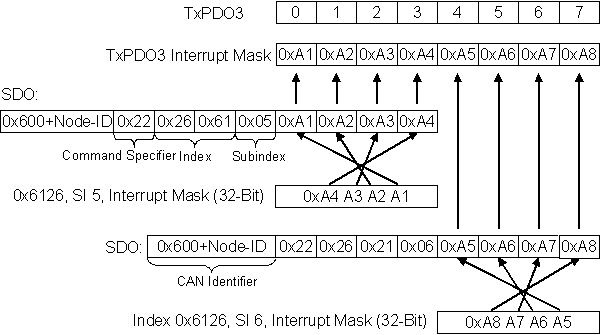
The value contained in a fast counter input is only to be transmitted when bits in the status word (the latch input, for instance) have changed. This requires the 32 bit counter value to be masked out (zeroed) in the interrupt mask. The status is located in byte 0, while the counter value is, by default, contained in bytes or 1..4 of the corresponding PDOs (TxPDO3 in this example, because < 65 digital and < 5 analog inputs are present).
This means that index 0x6126, subindex5 must receive the value 0x0000 00FF and that subindex6 must have 0xFFFF FF00 written into it.
The corresponding SDOs therefore appear as follows:
11-bit Identifier | 8-byte user data | |||||||
|---|---|---|---|---|---|---|---|---|
0x600+ Node-ID | 0x22 | 0x26 | 0x61 | 0x05 | 0xFF | 0x00 | 0x00 | 0x00 |
11-bit Identifier | 8-byte user data | |||||||
0x600+ Node-ID | 0x22 | 0x26 | 0x61 | 0x06 | 0x00 | 0xFF | 0xFF | 0xFF |
Digital outputs
Index | Subindex | Name | Type | Attribute | Mapping | Default value | Meaning |
|---|---|---|---|---|---|---|---|
0x6200 | 0 | Number of items | Unsigned8 | ro | N | Depending on type and fittings | Number of available digital 8-bit output data blocks |
1 | 1st input block | Unsigned8 | rw | Y | 0x00 | 1st output channel | |
... | ... | ... | ... | ... | ... | ... | |
0XFE | 254. input block | Unsigned8 | rw | Y | 0x00 | 254st output channel |
Analog inputs
Index | Subindex | Name | Type | Attribute | Mapping | Default value | Meaning |
|---|---|---|---|---|---|---|---|
0x6401 | 0 | Number of items | Unsigned8 | ro | N | Depending on type and fittings | Number of analog input channels available |
1 | 1st input | Unsigned16 | ro | Y | 0x0000 | 1st input channel | |
... | ... | ... | ... | ... | ... | ... | |
0XFE | 254. input | Unsigned16 | ro | Y | 0x0000 | 254st input channel |
The analog signals are displayed left aligned. The representation in the process image is therefore independent of the actual resolution. Detailed information on the data format can be found at the relevant signal type.
Analog outputs
Index | Subindex | Name | Type | Attribute | Mapping | Default value | Meaning |
|---|---|---|---|---|---|---|---|
0x6411 | 0 | Number of items | Unsigned8 | ro | N | Depending on type and fittings | Number of analog output channels available |
1 | 1st input block | Unsigned16 | rw | Y | 0x0000 | 1st output channel | |
... | ... | ... | ... | ... | ... | ... | |
0XFE | 254. input block | Unsigned16 | rw | Y | 0x0000 | 254st output channel |
The analog signals are displayed left aligned. The representation in the process image is therefore independent of the actual resolution. Detailed information on the data format can be found at the relevant signal type.
Event driven analog inputs
Index | Subindex | Name | Type | Attribute | Mapping | Default value | Meaning |
|---|---|---|---|---|---|---|---|
0x6423 | 0 | Global Interrupt Enable | Boolean | rw | N | FALSE (0) | Activates the event-driven transmission of PDOs with analog inputs. |
Although, in accordance with CANopen, the analog inputs in TxPDO2..4 are by default set to transmission type 255 (event driven), the event (the alteration of an input value) is suppressed by the event control in object 0x6423, in order to prevent the bus from being swamped with analog signals. It is recommended that the flow of data associated with the analog PDOs is controlled either through synchronous communication or through using the event timer. In event-driven operation, the transmission behavior of the analog PDOs can be parameterized before activation by setting the inhibit time (object 0x1800ff, subindex 3) and/or limit value monitoring (objects 0x6424 + 0x6425) and/or delta function (object 0x6426).
Upper limit value analog inputs
Index | Subindex | Name | Type | Attribute | Mapping | Default value | Meaning |
|---|---|---|---|---|---|---|---|
0x6424 | 0 | Number of items | Unsigned8 | ro | N | Depending on type and fittings | Number of analog input channels available |
1 | upper limit 1st input | Unsigned16 | rw | Y | 0x0000 | Upper limit value for 1st input channel | |
... | ... | ... | ... | ... | ... | ... | |
0XFE | upper limit 254. input | Unsigned16 | rw | Y | 0x0000 | Upper limit value for 254st input channel |
Values different from 0 activate the upper limit value for this channel. A PDO is then transmitted if this limit value is exceeded. In addition, the event driven mode must be activated (object 0x6423). The data format corresponds to that of the analog inputs.
Lower limit value analog inputs
Index | Subindex | Name | Type | Attribute | Mapping | Default value | Meaning |
|---|---|---|---|---|---|---|---|
0x6425 | 0 | Number of items | Unsigned8 | ro | N | Depending on type and fittings | Number of analog input channels available |
1 | lower limit 1st input | Unsigned16 | rw | Y | 0x0000 | Lower limit value for 1st input channel | |
... | ... | ... | ... | ... | ... | ... | |
0XFE | lower limit 254. input | Unsigned16 | rw | Y | 0x0000 | Lower limit value for 254st input channel |
Values different from 0 activate the lower limit value for this channel. A PDO is then transmitted if the value falls below this limit value. In addition, the event driven mode must be activated (object 0x6423). The data format corresponds to that of the analog inputs.
Delta function for analog inputs
Index | Subindex | Name | Type | Attribute | Mapping | Default value | Meaning |
|---|---|---|---|---|---|---|---|
0x6426 | 0 | Number of items | Unsigned8 | ro | N | Depending on type and fittings | Number of analog input channels available |
1 | delta value 1st input | Unsigned16 | rw | Y | 0x0000 | Delta value for the 1st input channel | |
... | ... | ... | ... | ... | ... | ... | |
0XFE | delta value 254. input | Unsigned16 | rw | Y | 0x0000 | Delta value for the 254st input channel |
Values different from 0 activate the delta function for this channel. A PDO is then transmitted if the value has changed by more than the delta value since the last transmission. In addition, the event driven mode must be activated (object 0x6423). The data format corresponds to that of the analog inputs (delta value: can only have positive values).