Register description
The registers can be read or written via the register communication. They are used for the parameterization of the terminal.
R0 to R7: Registers in the internal RAM of the terminal
The process variables can be used in addition to the actual process image. Their function is specific to the terminal.
- R0 ADC raw value (X_R)
This register contains the raw ADC value with gain and offset error
- R1 to R5: Reserved
- R6: Diagnostic register
- High byte: reserved
- Low byte: Status byte
- R7: Command register
High-Byte_Write = function parameter
Low-Byte_Write = function number
High-Byte_Read = function result
Low-Byte_Read = function number
R8 to R15: Registers in the internal ROM of the terminal
The type and system parameters are hard programmed by the manufacturer, and the user can read them but cannot change them.
- R8: Terminal type
The terminal type in register R8 is needed to identify the terminal.
- R9: Software version (X.y)
The software version can be read as a string of ASCII characters.
- R10: Data length
R10 contains the number of multiplexed shift registers and their length in bits.
The Bus Coupler sees this structure.
- R11: Signal channels
Related to R10, this contains the number of channels that are logically present. Thus for example a shift register that is physically present can perfectly well consist of several signal channels.
- R12: Minimum data length
The particular byte contains the minimum data length for a channel that is to be transferred. If the MSB is set, the control and status byte is not necessarily required for the terminal function and is not transferred to the control, if the Bus Coupler is configured accordingly.
- R13: Data type register
Data type register | Meaning |
|---|---|
0x00 | Terminal with no valid data type |
0x01 | Byte array |
0x02 | Structure 1 byte n bytes |
0x03 | Word array |
0x04 | Structure 1 byte n words |
0x05 | Double word array |
0x06 | Structure 1 byte n double words |
0x07 | Structure 1 byte 1 double word |
0x08 | Structure 1 byte 1 double word |
0x11 | Byte array with variable logical channel length |
0x12 | Structure 1 byte n bytes with variable logical channel length (e.g. 60xx) |
0x13 | Word array with variable logical channel length |
0x14 | Structure 1 byte n words with variable logical channel length |
0x15 | Double word array with variable logical channel length |
0x16 | Structure 1 byte n double words with variable logical channel length |
- R14: reserved
- R15: Alignment bits (RAM)
The alignment bits are used to place the analog terminal in the Bus Coupler on a byte boundary.
R16 to R30: Manufacturer parameter area (SEEROM)
The manufacturer parameters are specific for each type of terminal. They are programmed by the manufacturer, but can also be modified by the controller. The manufacturer parameters are stored in a serial EEPROM in the terminal, and are retained in the event of voltage drop-out.
These registers can only be altered after a code word has been set in R31.
- R17: Hardware compensation - offset (B_a)
KL3102: [approx. 0x00XX], KL3112 & KL3122 [0xFBxx]
16 bit signed integer*2^-16+1
This register is used for offset compensation of the terminal (Eq. 1.1).
- R18: Hardware compensation - gain (A_a)
KL3102: [approx. 0x24XX], KL3112 & KL3122 [0x48xx]
16 bit signed integer*2^-16+1
This register is used for gain compensation of the terminal (Eq. 1.1).
1 corresponds to 0x0000, 2 corresponds to 0xFFFF
- R19: Manufacturer scaling - offset (B_h)
16 bit signed integer [0x0000]
This register contains the offset of the manufacturer straight-line equation (equation 1.3). The straight-line equation is enabled via register R32.
- R20: Manufacturer scaling - gain (A_h)
KL3102: [0x0100], KL3112 and KL3122: [0x0000]
16 bit signed integer*2-8
This register contains the scale factor of the manufacturer's equation of the straight line (Eq. 1.3). The straight-line equation is enabled via register R32.
1 corresponds to register value 0x0400.
R31 to R47: User parameter area (SEEROM)
The user parameters are specific for each type of terminal. They can be modified by the programmer. The user parameters are stored in a serial EEPROM in the terminal, and are retained in the event of voltage drop-out. The user area is write-protected by a code word.
R31: Code word register in RAM
 | Functionality of the code word register The code word 0x1235 must be entered here so that parameters in the user area can be modified. If any other value is entered into this register, the write-protection is active. When write protection is not active, the code word is returned when the register is read. If the write protection is active, the register contains a zero value. |
- R32: Feature register
KL3102: [0x1106], KL3112 and KL3122[0x0002]
This register specifies the operation modes of the terminal. Thus, for instance, a user-specific scaling can be enabled for the analog I/Os.
| Value range of KL3112 and KL3122 For reasons of compatibility, 16 bits signed integer is selected as the (standard) output format. The positive value range for 0 mA / 4 mA to 20 mA therefore extends from 0 to 32767 (0x7FFF). This corresponds to 15 bits. Manufacturer scaling must be disabled in order to exploit all 16 bits of the terminal. |
Feature bit no. |
| Description of the operation mode |
|---|---|---|
Bit 0 | 1 | User scaling (R33, R34) active [0] |
Bit 1 | 1 | Manufacturer scaling (R19, R20) active [1] |
Bit 2 | 0 | Watchdog timer active [0] |
Bit 3 | 1 | Sign / amount representation [0] |
Bit 4…7 | - | Reserved, don't change |
Bit 9 | 1 | Limit value 1 active [0] |
Bit 10 | 1 | Limit value 2 active [0] |
Bit 11…15 | - | Reserved, don't change |
- R35: Limit value 1 (Y_2)
[0x0000]
If the process data are outside this threshold, the appropriate bits are set in the status byte.
- R36: Limit value 2 (Y_2)
[0x0000]
If the process data are outside this threshold, the appropriate bits are set in the status byte.
- R37: Filter constants of the A/D converter, and configuration bits for the filter
(default value: 35C0hex)
The terminal has two low-pass filter stages: - The first stage consists of a sinc3 filter, and is always active.
- The second stage consists of a 22nd order FIR filter. This can be deactivated.
Bit | 15 | 14 | 13 | 12 | 11 | 10 | 9 | 8 | 7 | 6 | 5 | 4 | 3 | 2 | 1 | 0 |
Name | Filter constant Nf (Nf.11 to Nf.0) | Zero | Zero | Skip | Fast | |||||||||||
Notes on the filter
The filter architecture of the KL31x2 is as follows:
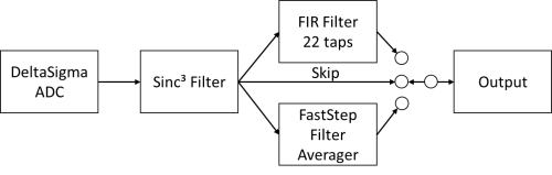
- he Sinc³ is always active
- In step 2 you can select
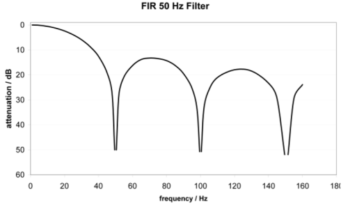
- The variable FIR filter. It is a notch filter, configuration parameter is here the first notch frequency, which is almost completely attenuated, just like the multiples of it.
The -3dB frequency is therefore considerably higher. A typical attenuation curve: - Alternatively, the FastStep Filter can be used. Despite a normally active FIR filter stage, there is a fast reaction to jumps at the input: if a fast level change of >1% of the measuring range between 2 samples is detected, the FastStep automatically switches to a self adjusting average filter for a short time and then back to the FIR filter.
Signal changes can be monitored quickly in this way. - Or no second filter is used via "Skip" and only the sinc³ filter is active.
Bit | Name | Description | Default |
|---|---|---|---|
R37.15 | Filter constant Nf | The filter constant Nf specifies the 3dB limit frequency of the sinc3 filter. The value ranges from 150 to 2047. | 35Chex (860dec) |
... | |||
R37.4 |
| Skip = 0 | Flimit = 11981 / Nf |
|
| Fstop = 43008 / Nf |
| Skip = 1 | Flimit = 81076 / Nf |
Bit | Name | Description | Default | |
|---|---|---|---|---|
R37.3 | Zero | 0bin | See note below | 0bin |
R37.2 | Zero | 0bin | 0bin | |
| Do not change Bits R37.2 and R37.3 must always be ZERO, otherwise errors will occur in the A/D converter! |
Bit | Name | Description | Default | |
|---|---|---|---|---|
R37.1 | Skip | 0bin | FIR filter is enabled. | 0bin |
1bin | FIR filter is bypassed. | |||
R37.0 | Fast | 0bin | Fast Step Mode and FIR filter are disabled. | 0bin |
1bin | Fast Step Mode and FIR filter are active | |||
Examples
Attention, the upper 3 digits of the value in R37 in hex are the filter constant, the 4th digit is the skip/fast step setting.
Value in R37 | Fstop | Cycle time |
|---|---|---|
0x35C0 | 50 Hz | 140 ms |
0x2660 | 70 Hz | 100 ms |
0x1330 | 140 Hz | 50 ms |
0x7FF1 (Fast-Step activated) |
| 40 ms |
0x3FF1 (Fast-Step activated) |
| 20 ms |
0x1001 (Fast-Step activated) |
| <4 ms |
Value in R37 | Flimit | Cycle time |
|---|---|---|
0x7FF2 (Skip mode, only sinc³ active) | 39.6 Hz | 40 ms |
0x3FF2 (Skip mode, only sinc³ active) | 77.36 Hz | 20 ms |
0x1002 (Skip mode, only sinc³ active) | 158 Hz | <4 ms |